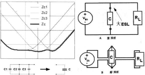
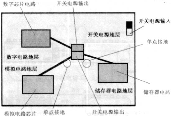
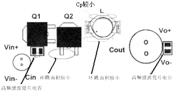
Nowadays, since the switching power supply generates electromagnetic waves and affects the normal operation of its electronic products, the correct power PCB layout technology becomes very important. This article refers to the address: http:// In many cases, a power supply that is perfectly designed on paper may not work properly during initial commissioning because of the many problems with the PCB layout of the power supply. For example, a buck switching power supply on a consumer electronics device. In terms of schematics, the designer should be able to distinguish between the components in the power circuit and the components in the control signal circuit on this circuit diagram, but if the designer treats all the components in the power supply as components in the digital circuit. Processing, the problem will be quite serious. Switching power supply PCB layout is completely different from digital circuit PCB layout. In digital circuit layout, many digital chips can be automatically arranged by PCB software and the connections between the chips can be automatically connected by PCB software. The switching power supply formatted by the automatic typesetting method certainly cannot work normally. Therefore, designers need to master and understand the correct switching power supply PCB layout technical rules. Switching power supply PCB layout technical rules The capacitance of the bypass ceramic capacitor should not be too large, and its parasitic series inductance should be minimized. Multiple capacitors in parallel can improve the high frequency impedance characteristics of the capacitor When a capacitor operating frequency is below fo, the capacitor impedance Zc decreases with increasing frequency; when the capacitor operating frequency is above fo, the capacitor impedance Zc will increase as the inductor impedance increases with frequency; when the capacitor works When the frequency is close to fo, the capacitor impedance is equal to its equivalent series resistance (RESR). Electrolytic capacitors generally have large capacitance and large equivalent series inductance. Because of its low resonant frequency, it can only be used on low frequency filtering. Tantalum capacitors generally have larger capacitance and smaller equivalent series inductance, so their resonant frequency will be higher than electrolytic capacitors and can be used in medium and high frequency filtering. The capacitance of the ceramic capacitor and the equivalent series inductance are generally small, so its resonant frequency is much higher than that of electrolytic capacitors and tantalum capacitors, so it can be used in high frequency filtering and bypass circuits. Since the resonant frequency of a small-capacity ceramic chip capacitor is higher than the resonant frequency of a large-capacity ceramic chip capacitor, When selecting a bypass capacitor, it is not possible to use a ceramic capacitor with a high capacitance value. In order to improve the high-frequency characteristics of the capacitor, a plurality of capacitors of different characteristics can be used in parallel. Fig. 1(a) is an improved impedance effect after a plurality of capacitors of different characteristics are connected in parallel. It is not difficult to understand the importance of this typesetting rule through analysis. Figure 1(b) shows the different traces of the input power (VIN) to load (RL) on a PCB. In order to reduce the ESL of the filter capacitor (C), the lead length of the capacitor leads should be as short as possible: and the traces from VIN positive to RL and VIN negative to RL should be as close as possible. Figure 1 (a) Multiple capacitors in parallel to improve impedance characteristics Figure 1 (b) Filter circuit PCB trace mode A is poor, B is good The parasitic shunt capacitance of the inductor should be minimized, and the distance between the inductor pins should be as far as possible. The current loop in Figure 2(a) is similar to the inductance of only one coil winding. It can be seen that the electromagnetic field B(t) generated by the high frequency alternating current will surround the outside and inside of the loop. If the high-frequency alternating current loop area (Ac) is large, large electromagnetic interference will occur inside and outside the loop. Figure 2(a) shows that the current loop is similar to an inductor with only one coil winding. When the operating frequency of an inductor is below fo, the impedance of the inductor increases with the increase of frequency; when the operating frequency of the inductor is above fo, the impedance of the inductor decreases with increasing frequency; when the operating frequency of the inductor is close to fo, the impedance of the inductor is equal to Its equivalent parallel resistance (REPR). In the application of switching power supplies, the equivalent parallel capacitance (CP) of the inductor should be controlled as small as possible. At the same time, it must be noted that the inductance of the same inductance will produce different equivalent parallel capacitance values ​​(CP) due to different coil configurations. Figure 2(b) shows the equivalent parallel capacitance values ​​for the inductors of the same inductance under two different coil configurations. The five-turn winding of the first inductor in Figure 2(b) is wound in sequence. The equivalent parallel capacitance value (CP) produced by this coil structure is one-fifth of the equivalent parallel capacitance value (C) of a single set of coils. The five-turn winding of the second inductor in Figure 2(b) is wound in a cross-over sequence. Where windings #4 and #5 are placed between winding #1#2#3 and windings #1 and #5 are very close. The equivalent parallel capacitance value (Cp) produced by this coil structure is equivalent parallel connection of a single set of coils. The capacitance value (C) is twice. It can be seen that the equivalent parallel capacitance values ​​of the two inductors of the same inductance actually differ by a factor of ten. In high-frequency filtering, if the equivalent parallel capacitance of an inductor is too large, high-frequency noise can easily flow directly to the load through its parallel capacitor. Such an inductor also loses its high frequency filtering function. Figure 2(b) Different equivalent parallel capacitance values ​​due to different coil configurations Figure 2(c) shows the different traces of the input power (VIN) through the inductor (L) to the load (RL) on a PCB. In order to reduce the Cp of the inductor, the two pins of the inductor should be kept as far as possible. The trace from VIN positive to RL and VIN negative to RL should be as close as possible. Figure 2 (c) Filter circuit PCB trace mode A difference B is good Avoid placing any power or signal traces on the formation. The graph A in Fig. 3(a) is a scenario when a direct current flows over a ground plane. At this time, the returning direct current on the formation is distributed very evenly over the entire ground level. Figure B in Figure 3(a) shows the scenario when high frequency alternating current flows over the same formation. At this point, the returning alternating current on the formation can only flow in the middle of the ground level and there is no current at all on the ground level. Assuming that the ground plane in Figure 3(b) is the Ground Plane on the switching power supply PCB, designers should try to avoid placing any power or signal traces on the ground plane. Once the traces on the formation destroy the entire high-frequency AC loop, the circuit generates very human electromagnetic radiation that disrupts the normal operation of the surrounding electronics. Figure 3 (a) Mirror surface concept A DC B AC Figure 3 (b) Ground layer damage caused by traces on the ground plane The area of ​​the high frequency AC loop should be minimized In order to reduce the electromagnetic wave noise generated by the high frequency AC loop, the area of ​​the loop should be controlled to be very small. As shown in Fig. 4, if the area AC of the high-frequency alternating current loop is large, large electromagnetic interference occurs inside and outside the loop. If the same high-frequency AC current is used, when the loop area is designed to be very small, the internal and external electromagnetic fields of the loop cancel each other out, and the entire circuit becomes very quiet. Figure 4 high frequency AC loop Via placement should not destroy the path of high frequency AC current on the formation Many designers prefer to place many vias (VIAS) on a multi-layer PCB. However, it is necessary to avoid placing too many vias on the high frequency AC current return path. Otherwise, the high-frequency AC current traces on the formation will be destroyed. If some vias must be placed on the high-frequency AC current path, some space can be left between the vias for the high-frequency AC current to pass smoothly. Figure 5(a) shows the way the vias are placed. Designers should also be aware that different pad shapes will produce different series inductances. Figure 5(b) shows the series inductance values ​​for several pad shapes. The placement of the bypass capacitor (Decouple) also takes into account its series inductance value. The bypass capacitor must be a low impedance and low ESL ceramic capacitor. But if a high-quality ceramic capacitor is placed on the PCB in a wrong way, its high-frequency filtering function will disappear. Figure 5(c) shows the correct and incorrect placement of the bypass capacitor. Figure 5 (a) Via placement method Figure 5 (b) Pad parasitic series inductance Figure 5 (c) Bypass capacitor correct and incorrect placement Power supply DC output Many switching power supplies are loaded away from the output port of the power supply. In order to avoid the output traces being disturbed by electromagnetic waves generated by the power supply itself or peripheral electronics, the output power traces must be close together as shown in Figure 6. The area of ​​the output current loop must also be reduced. Figure 6 power output DC current loop Different circuits on the system board require different ground planes. The ground planes of different circuits are connected to the power ground plane through a single point. Analog circuits, digital circuits, and switching power supply circuits are available on the next-generation electronics system board. In order to reduce the effects of switching power supply noise on sensitive analog and digital hand circuits, it is often necessary to separate the ground planes of the different circuits. If a multilayer PCB is selected, the ground planes of the different circuits can be separated by different PCB layers. If the entire product has only one ground plane, it must be separated in a single layer as in Figure 7. Whether layer separation on a multilayer PCB or formation separation on a single-layer PCB, the formation of different circuits should be connected to the ground of the source in the switch by a single point. Figure 7 Single-store connection of circuit ground plane and power ground plane Switching power supply PCB layout technical rules application examples Return to the schematic diagram of the switching power supply of Figure 8 (a); usually first need to know the path of the high-frequency AC current of the power supply, and can distinguish between the small-signal control circuit and the power circuit components and their wiring, Figure 8 (a) will be the traditional power supply The schematic (ie, a circuit diagram without thick black lines) is divided into a control circuit portion and a power circuit portion. Generally speaking, the power circuit of the power supply mainly includes an input filter capacitor, an output filter capacitor, a filter inductor, and an upper and lower power FET. The control circuit mainly includes a PWM control chip, a bypass capacitor, a bootstrap circuit, a feedback voltage dividing resistor, and a feedback compensation circuit. Figure 8 (a) Power control circuit (thin line) and power circuit (thick line) Power supply circuit PCB layout Proper placement and routing of power supply devices on the PCB will determine if the entire power supply is working properly. Figure 8(b) shows the current and voltage waveforms on a buck switching power supply power circuit component. Since the current flowing from the input filter capacitor (CIN), the upper FET (Q1) and the lower FET (Q2) is an AC current with high frequency and high peak, it is used by CIN-Q1-Q2. The loop area formed should be minimized. At the same time, the loop area composed of the lower field effect transistor (Q2), the inductor (L), and the output filter capacitor (Cout) also needs to be minimized. Figure 8(b) Current and voltage on the switching power supply power circuit If the power circuit PCB is not fabricated in accordance with the above-mentioned points of the PCB layout technical rules, it is possible to produce a power supply PCB with many errors. Figure 8 (c) is a better power supply circuit PCB trace. Figure 8(c) Proper switching power supply power device placement and routing The area of ​​the CIN-Q1-Q2 and Q2-L-Cout loops has been controlled to a minimum. The source of the upper FET (Q), the junction between the drain of the lower FET (Q2) and the output inductor (L) is a single copper pad. Since the voltage at this connection point is high frequency and AC, Q1 and Q2 and B need to be very close. Although there is no high-frequency alternating current in the trace between the output filter inductor (L) and the output filter capacitor (Cout), a wider trace can reduce the loss of the DC impedance and improve the efficiency of the power supply. If cost permits, the power supply can be used on a double-sided PCB that is completely grounded on one side. But care must be taken to avoid running power and signal lines on the ground. A ceramic capacitor is added to the input and output ports of the power supply to improve the high frequency filtering of the power supply. Power control circuit PCB layout The power control circuit PCB layout technical rule should be as short as possible to control the drive circuit loop of the chip to the upper and lower FETs. Power control circuit PCB layout is also very important. Unreasonable typesetting can cause drift and oscillation of the power supply output voltage. The control line should be placed on the side of the power circuit and must never be placed in the middle of the high frequency AC loop. The bypass capacitor should be as close as possible to the chip's Vcc and ground pin (GND). The feedback divider resistor is also preferably placed near the chip. The loop that drives the chip to the FET should also be as short as possible. Conclusion The above-mentioned typographic technical rules of the switching power supply PCB layout should be gradually mastered and applied in practice, so that the high quality of the designed portable switching power supply conforms to the portable electronic system.
FGI `s Distribution Transformers have the characteristics of low empty load loss and low operating cost. The positioning and connection of the body is firm, so the effective protection of Distribution Transformer is greatly enhanced. The overall structure is superior, the electrical performance is good, and the product reliability is high. The National Transformer Quality Supervision and Inspection Center passed all the tests for FGI `s electricity transformers including short-circuit withstand capability. The type of transformer contains Oil Immersed Power Transformer and Dry Type Transformer.
Distribution Transformers Distribution Transformer,Electrical Distribution Transformers,Power Distribution Transformer,Distribution Transformers Abb,Distribution Transformers Connections FGI SCIENCE AND TECHNOLOGY CO., LTD , https://www.fgi-tech.com