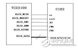
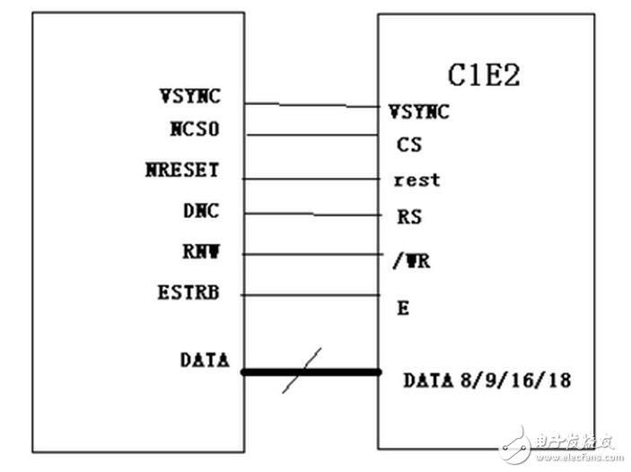
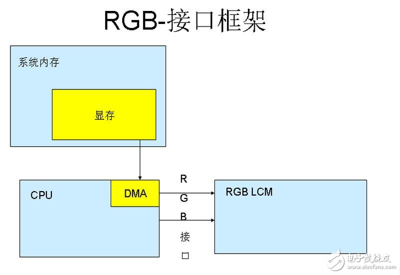
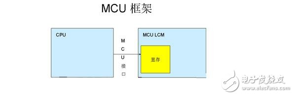
There are many types of LCD interfaces, and the classification is very fine. Mainly look at the LCD drive mode and control method, currently there are several types of color LCD connection on the phone: MCU mode, RGB mode, SPI mode, VSYNC mode, MDDI mode, DSI mode. MCU mode (also written in MPU mode). Only the TFT module has an RGB interface. However, the application is more MUC mode and RGB mode, the difference is as follows: 1. MCU interface: The command will be decoded, and the timing signal will be generated by the TIming generator to drive the COM and SEG drivers. RGB interface: When writing LCD register setTIng, there is no difference between the MCU interface and the MCU interface. The only difference is the way the image is written. 2. In the MCU mode, since the data can be stored in the internal GRAM of the IC and then written to the screen, this mode LCD can be directly connected to the MEMORY bus. It is different when using RGB mode. It has no internal RAM. HSYNC, VSYNC, ENABLE, CS, RESET, RS can be directly connected to the GPIO port of MEMORY, and the waveform is simulated with GPIO port. 3. MPU interface mode: display data is written to DDRAM, which is often used for still picture display. RGB interface mode: display data is not written to DDRAM, direct write screen, fast, often used for displaying video or animation. The main differences between the MCU interface and the RGB interface are: MCU interface mode: Display data is written to DDRAM, which is often used for still picture display. RGB interface mode: display data is not written to DDRAM, direct write screen, fast, often used for displaying video or animation. Because it is mainly used in the field of microcontroller, it is named. After the heavy use of low-end mobile phones, its main features are cheap. The standard terminology of the MCU-LCD interface is Intel's 8080 bus standard, so I80 is used to refer to the MCU-LCD screen in many documents. Mainly can be divided into 8080 mode and 6800 mode, the main difference between the two is timing. Data bit transmission has 8 bits, 9 bits, 16 bits, 18 bits, and 24 bits. The connection is divided into: CS/, RS (register selection), RD/, WR/, and then the data line. The advantage is that the control is simple and convenient, and no clock and synchronization signals are needed. The disadvantage is that it costs GRAM, so it is difficult to achieve a large screen (3.8 or above). For the LCM of the MCU interface, the internal chip is called the LCD driver. The main function is to transform the data/command sent by the host into RGB data of each pixel and display it on the screen. This process does not require point, line, or frame clocks. The Driver IC of the LCD of the MCU interface is equipped with GRAM. The Driver IC acts as a coprocessor of the MCU and accepts the Command/Data sent by the MCU, which can work relatively independently. For the LCM (LCD Module) of the MCU interface, the internal chip is called the LCD driver. The main function is to transform the data/command sent by the host into RGB data of each pixel and display it on the screen. This process does not require point, line, or frame clocks. The M6800 mode supports an optional bus width of 8/9/16/18-bit (default is 8 bits). The actual design idea is the same as the I80. The main difference is that the bus control read/write signals of this mode are combined. One pin (/WR) is added with a latch signal (E) and the data bit is transmitted with 8 bits, 9 bits, 16 bits and 18 bits. The I80 mode connection is divided into: CS/, RS (register selection), RD/, WR/, and then the data line. The advantage is that the control is simple and convenient, and no clock and synchronization signals are needed. The disadvantage is that it costs GRAM, so it is difficult to achieve a large screen (QVGA or higher). The standard name of the MCU interface is I80, and there are five control pins for the pin: RS (set 1 to write data, set 0 to write command) /WR (0 means write data) Data command distinguishes signal RESET reset LCD (reset with fixed command series 0 1 0) This mode is actually adding a VSYNC signal to the MCU mode, which is applied to the motion picture update, which is very different from the above two interfaces. This mode supports direct animation display, which provides a minimal change to the MCU interface and an animation display solution. In this mode, the internal display operation is synchronized with the external VSYNC signal. Animated display at a higher rate than internal operations can be achieved. However, due to the different modes of operation, this mode has a limitation on the rate, that is, the write rate to the internal SRAM must be greater than the rate at which the internal SRAM is read. The large screen adopts more modes, and the data bit transmission also has 6 bits, 16 bits and 18 bits, and 24 bits. Connections generally include: VSYNC, HSYNC, DOTCLK, CS, RESET, and some also require RS, and the rest is the data line. Its advantages and disadvantages are exactly the opposite of the MCU mode. The main difference between the MCU-LCD screen and the RGB-LCD screen is the location of the memory. RGB-LCD memory is played by system memory, so its size is only limited by the size of the system memory, so RGB-LCD can make larger sizes, like 4.3" now only "entry level, and MID 7" The 10" screens are used in large quantities. The design of the MCU-LCD is as long as the memory of the microcontroller is small, so the memory is built into the LCD module. Then the software updates the memory by special display commands, so the MCU screen It can't be done very much. At the same time, the display update speed is slower than RGB-LCD. The display data transmission mode is also different. The RGB screen only needs to store and organize the data. After the display is started, the LCD-DMA will automatically pass the data in the memory to RGB. The interface is sent to the LCM, and the MCU screen needs to send a command to draw the MCU's internal RAM (that is, it cannot directly write the RAM of the MCU screen). Therefore, the RGB display speed is obviously faster than the MCU, and the MCU-LCD is also used for playing video. slower. For the LCM of the RGB interface, the output of the host is directly the RGB data of each pixel, and no conversion is required (except GAMMA correction, etc.). For this interface, an LCD controller is required in the host part to generate RGB data and Point, line, and frame sync signals. Color TFT LCD screens mainly have two kinds of interfaces: TTL interface (RGB color interface), LVDS interface (package RGB color into differential signal transmission). The TTL interface is mainly used for small-size TFT screens of 12.1 inches. The LVDS interface is mainly used for large-size TFT screens of 8 inches or more. There are many TTL interface lines and short transmission distances; the LVDS interface has a long transmission distance and a small number of lines. The large screen uses more modes, the control pins are VSYNC, HSYNC, VDEN, VCLK, S3C2440 supports up to 24 data pins, and the data pin is VD[23-0]. The image data sent by the CPU or graphics card is a TTL signal (0-5V, 0-3.3V, 0-2.5V, or 0-1.8V), and the LCD itself receives the TTL signal, because the TTL signal is transmitted at a high rate over a long distance. Poor performance, poor anti-interference ability, and later proposed a variety of transmission modes, such as LVDS, TDMS, GVIF, P&D, DVI and DFP. They actually only encode the TTL signal from the CPU or graphics card into various signals for transmission, and decode the received signal on the LCD side to get the TTL signal. But regardless of the transmission mode, the essential TTL signal is the same. Note: TTL/LVDS are the transmission modes of two kinds of signals respectively. TTL is high level means 1 and low level means 0 mode. LVDS is positive and negative two corresponding waveforms. The difference between two waveforms is used to indicate that it is currently 1 or 0 It is used less, there are 3 lines and 4 lines, the connection is CS/, SLK, SDI, SDO four lines, the connection is small but the software control is more complicated. MDDI mode (MobileDisplayDigitalInterface) Qualcomm's interface MDDI, proposed in 2004, improves mobile phone reliability and reduces power consumption by reducing connectivity, which will replace SPI mode and become a high-speed serial interface for mobile. The connection is mainly host_data, host_strobe, client_data, client_strobe, power, GND several lines. This mode serial bidirectional high-speed command transmission mode, the connection has D0P, D0N, D1P, D1N, CLKP, CLKN. How to see the type of microcontroller from the LCD electrode: Picking up the measured signal through the measuring instrument is a commonly used data acquisition method in the forward channel design of the single chip microcomputer. Usually, the interface circuit obtains the relevant analog signal from the instrument circuit, and sends it to the single-chip microcomputer through A/D conversion or V/F conversion; or obtains a frequency signal, which is sent to the single-chip microcomputer after being shaped. However, such signals may not be found in some meter circuits. Taking a capacitive pressure sensor sphygmomanometer as an example, although a frequency signal linearly related to the pressure can be obtained from the oscillating circuit and sent to the single-chip microcomputer to measure the pressure, the pressure is not the systolic pressure, diastolic pressure and heart rate to be picked up. The ordinary sphygmomanometer does not have a communication interface like a smart meter to communicate with the microcontroller. Obviously, in order to pick up the signal under test through such a meter, only the reading of its display screen is directly read. This article takes an automatic sphygmomanometer as an example to introduce the interface circuit for reading the LCD display reading into the MCU. The sphygmomanometer display is a 61/2-segment LCD display with 3 digits showing systolic pressure and 3 digits showing diastolic pressure. The l/2 bit is in the middle of the two sets of numbers and displays four indicators. 1 is an electrode connection structure and an equivalent circuit of a sphygmomanometer LCD. 1(a) is a common electrode connection arrangement, and FIG. 1(b) is a segment electrode connection arrangement. It has 4 common electrodes COM0~COM3, each of which has 2 segment electrodes Sx-0, Sx-1, and its equivalent circuit is a matrix of 4 rows & TImes; 2 columns, as shown in Figure l(c) . Observe the working waveform of the sphygmomanometer LCD with a dual trace oscilloscope, as shown in Figure 2. It is driven by the time division drive method, with a ratio of 1/3, a duty ratio of l/4, and a B type. The signal waveforms of the common electrodes COM0 to COM3 are always kept constant, and the waveforms of the segment electrodes Sx-0 and Sx-1 vary with the display number. The Sx-1 and Sx-1 waveforms in Fig. 2 are the operating waveforms when the number "O" is displayed. As can be seen from FIG. 2, regardless of the DC component of the signal, the first half periods t1 to t4 of all the waveforms are equal in magnitude to the second half period t5 to t8, and the polarities are opposite. The signal voltages of COM0 to COM3 sequentially reach peak values ​​in four times from t1 to t4. The time t1 is the scanning time of the two segments f and a on the first row, the common electrodes COM0, Sx-0 are segment electrodes of the f segment, and Sx-1 is the segment electrode of the segment a. During the time t1, the voltage COM0-Sx-0=V0 on the f-segment, the voltage COM0-Sx-1=V0 on the a-segment, both f and a are in the selected state and displayed. The voltages and display states of the remaining segments during their scan time are listed in Table 1. In the 7-segment, only the voltage on the g segment is V0/3, which is in the non-selected state and is not displayed. The remaining 6 segments are in the selected state and displayed. Therefore, the number "O" is displayed. It can be seen that the voltage COMx-Sx-y (x=0,1,...,6;y) on each segment of f, a, g, b, e, c, and d in four times t1 to t4 is sequentially checked. =O,1) Whether it is V0 or V0/3, the glyph codes of the LCD digits can be obtained, and then the glyph codes are converted into measurement results. Figure 3 is an 805l single-chip reading interface circuit designed according to the above working principle. In the figure, the LCD is a liquid crystal display of a sphygmomanometer. The 6-digit numbers are numbered O~5 from right to left, and the middle half is numbered 6. It has 13 segment electrodes, 4 COM electrodes, and GND is the ground terminal of the sphygmomanometer. The PC port of the 805l is an extended parallel port of the 805l. The display state reading circuit is composed of CD4067, CD3405l, LM324 (UA, UB), and the display state of each segment of the LCD digital is read. The CD41367 multi-channel analog switch selects one Sx-x output from the 13 segment electrode signals of the LCD to the inverting input terminal 2 of the LM324 (UA). The CD405l multi-channel analog switch selects one COMx output from the four COM signals of the LCD to the non-inverting input terminal 3 of the LM321 (UA). The LM324 (UA) is connected to the analog subtractor, and the signal COMx-Sx-x is output by the 1-pin. UB is used as a voltage comparator. The reference voltage VR is adjusted by potentiometer W1 between V0/3 and V0, and the segment voltage COMx-Sx-x is compared with VR. The comparison result is the display state of the segment, the high level indicates the segment display, and the low level is not displayed. The display status is fed into the P1.6 pin of the 8051. R1 and C1 form an RC filter to filter out high frequency interference. For example, to read the display state of the a-segment of the 0th digit, as shown in Fig. 1, the segment electrode of the digital a segment of the 0th is S0-1, and the common electrode is COM0. It is controlled by the program to make PC1PC0=00 in t1 time, make CD405l select COM0, make PC5~PC2=0001, make CD4067 select S0-1, COM0 and S0-1 signal voltages are subtracted by UA subtractor, then UB After the voltage comparison, the display state of the a segment is obtained, and the 8051 reads the most displayed state from the P1.6 pin. UC and UD form an INT0 interrupt signal generation circuit. The UC is connected to a voltage follower to reduce the effect of the circuit on the COM0 signal. R2 and C2 form an RC filter to filter out high frequency interference. UD is used as a voltage comparator, the reference voltage VR is added to the non-inverting input terminal, and the VR size is adjusted by the potentiometer W2 to 2V0/3 to V0. The voltage comparator converts the COM0 signal into an INT0 negative pulse signal, and the operating waveform is as shown in FIG. The falling edge of the negative pulse is the start time of the LCD drive signal period T. This negative pulse is connected to the INT0 pin of the 8051, which generates an external interrupt 0 on the falling edge of the negative pulse. Enable external interrupt 0 and timer T0 to read the glyph codes of the LCD digits in interrupt mode. The main program reads the glyph code by query, and then converts the glyph code into a reading after the reading check, the glyph code to the BCD code decoding, the reading recognition, and the like. The glyph code of a certain number of LCD is read by an external interrupt O and a timer T0 in an interrupted manner. As shown in Figure 5, the INT0 negative pulse causes an external interrupt O at the beginning of the period T, and the T0 timer is started by the INT0 interrupt service routine, f, a, g, b, e in the half cycle from t1 to t4. Each of c, d generates a T0 interrupt, reads the display state of each segment, and obtains a glyph code. The T0 timer is set to the operating mode 2, the automatic reloading timing is T/16, and the initial timing is T/32. The INT0 and T0 interrupt service routines are shown in Figure 6. Among them, PC port data format: PC5 ~ PC3 is the LCD digital number to be read, PC2 is the segment electrode number, PC1PC0 is the COM electrode number. The main program reads the glyph codes of the digits collected by the interrupt service program in a query manner, and the table table converts the glyph codes into BCD codes, and then converts the digital BCD codes into numerical values. It takes 1 cycle T to read a digital glyph code (actually only the first half cycle), measured, T = 16.318 ms. It takes at least 7 cycles to read all the digits, about 114ms. Taking into account that during the reading of the microcontroller, the LCD reading may change and the reading is wrong. The program uses two consecutive readings to verify the correctness of the reading. If the two consecutive readings are the same, the reading is correct; if the two consecutive readings are different, the reading may be wrong and should be read again. In addition to systolic blood pressure, diastolic blood pressure and heart rate, the sphygmomanometer also has instantaneous pressure during inflation and deflation, as well as some status information. The half position (No. 6) in the middle of the LCD is used to display four symbols of Reay to measure, CUFF Inf1aTIng, CUFF Deflating, and Replace Battcries. In addition, when the number 4 is displayed as "E", the measurement error is displayed. When "P" is displayed, the number displayed on the right 3 digits (0 to 2) is the heart rate. When the content on both the left and the right is a number, the left 3 digits (3 to 5) are systolic blood pressure, and the right 3 digits are diastolic pressure. Blood pressure and heart rate alternate. The main program uses this information to identify what the LCD displays. Use this interface circuit to collect data without having to consider the details and specifications associated with the measurement of the picked up signal. Thus, when the measurement of the pickup signal is complicated, the development cycle can be effectively shortened. At the same time, it does not have the problem that the data collected by the single-chip microcomputer and the meter reading are not completely consistent in the secondary A/D conversion or V/F conversion method. The program design reads a 1-digit number with one drive signal cycle. This read speed is sufficient for a sphygmomanometer whose reading changes are not very fast. If the LCD reading of the measuring instrument changes rapidly, you can modify the programming, read several digits simultaneously in one cycle, or even modify the circuit design, and use the second half cycle for reading, so that all the signals are read in one signal cycle. Digital. Turn on the multimeter and connect to the resistor file. It is best to have a buzzer. A pen touches the antenna casing of the set-top box, and a pen gradually releases each needle. When a drop appears, the test pen does not leave. It always sounds long. The needle is ground (GND), and the other needles continue to be measured. The short corner of the needle corner is VCC. This determines the GND and VCC. The remaining two pins of the three pins are RX and TX. The remaining two needles of the same four needles are also RX and TX. The five-pin judgment is to turn the multimeter to 20V, one to GND, and a step-by-step voltage. There are two situations at this time. The first one: there may be almost no voltage. At this time, when you look at the board and find two patch-level three-stage tubes near the pin holder, consider using the 2-2-3 RS232 serial port to connect. It is. Second, the five-pin voltage is measured to remove the highest and lowest voltage two pins, the rest are RX and TX. Because the highest voltage is VCC is low BT /RD (0 means read data)
57 Jack.China RJ11 Jack 1X5P,RJ11 Connector with Panel supplier & manufacturer, offer low price, high quality 4 Ports RJ11 Female Connector,RJ11 Jack 6P6C Right Angle, etc.
The RJ-45 interface can be used to connect the RJ-45 connector. It is suitable for the network constructed by twisted pair. This port is the most common port, which is generally provided by Ethernet hub. The number of hubs we usually talk about is the number of RJ-45 ports. The RJ-45 port of the hub can be directly connected to terminal devices such as computers and network printers, and can also be connected with other hub equipment and routers such as switches and hubs.
RJ11 Jack 1X5P,RJ11 Connector with Panel,4 Ports RJ11 Female Connector,RJ11 Jack 6P6C Right Angle ShenZhen Antenk Electronics Co,Ltd , https://www.pcbsocket.com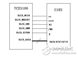
What are the LCD interfaces?