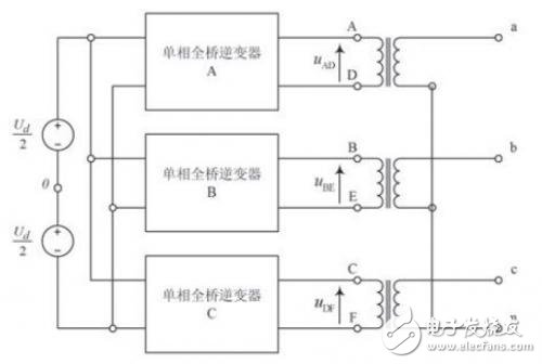
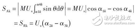
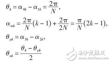
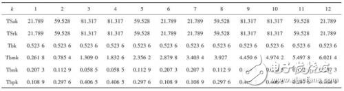
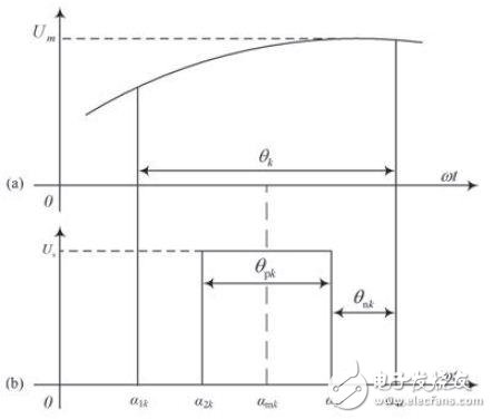
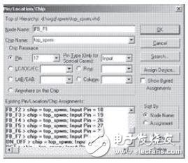
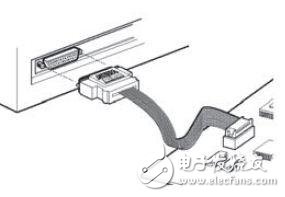
At present, the types of aviation power supply are different and the types are complex. It should be said that the comprehensive performance is not high enough. Especially with the continuous development of aircraft, its power supply protection needs to face many new challenges. Therefore, the development of advanced power supply protection equipment, improve its versatility and comprehensiveness, can provide universal support for the existing types of aircraft, not only can adapt to the needs of aircraft replacement, improve its practicality, and can compress the number of equipment and equipment. scale. The research case is an aviation inverter power supply, which is characterized by the fact that the amplitude and phase of the three-phase Voltage are always balanced under the premise of load three-phase balance. The combined three-phase full-bridge inverter circuit is shown in Figure 1. This paper introduces the technology modern electronic design automation technology (EDA), which integrates very high-speed integrated circuit hardware description language design language (VHDL) and programmable logic circuit (PLD). The components are designed and implemented with control logic, and the combined three-phase inverter circuit is controlled to obtain the required output voltage and waveform. Design and calculation of a sinusoidal pulse width modulation scheme Pulse-width Modula (PWM) is a series of pulse widths designed at a fixed frequency to control the on and off states of the switching devices of the inverter, and obtain the required aviation power at the output to meet the design. Quality requirements. 1.1 Mathematical model of the equivalent area method The equivalent area sinusoidal pulse width modulation (SPWM) generation method is adopted, which has the advantages of small harmonic output waveform, close to sinusoidal waveform and simple algorithm. First, the ideal sine wave is divided into several equal parts. As shown in Fig. 2, the area formed by an aliquot of the arc and the time axis is equivalent to a rectangular pulse width, provided that the center of the rectangular pulse width and the center of the arc projection The points coincide on the time axis, and the two areas are equal. The larger the number of divided aliquots, the closer the entire rectangular pulse series is to the ideal sinusoidal waveform required for the design. The rectangular pulse width is used to control the inverter. The on and off states of the components. Figure 1 schematic diagram of combined inverter circuit For example, for the kth pulse, the sinusoidal waveform arc forms an area perpendicular to the time axis and SAK, and the equivalent pulse rectangle area is SRk, which is easy to get: Where: the modulation parameter is M; the ideal sine wave is divided into N equal parts. The time width of each aliquot is θk, the midpoint of the time axis of each aliquot is αmk, the rectangular width of the equivalent area (corresponding to the conduction time) is θpk, and the remaining time of the rectangle at the opposite ends of the equivalent area (equivalent to the cutoff The time) is θnk and the calculation formula is: 1.2 Design calculation and data generation After setting a certain value, the numerical calculation is performed by the mathematical tool Matlab software through the above equations and formulas, and the table 1 and the pulse data are generated. Table 1 pulse series data Figure 2 equivalent area algorithm SPWM generation model 2 software and hardware design and implementation 2.1 software design and implementation The hardware of the control circuit adopts PLD components, and is designed based on VHDL language to achieve the required logic functions to achieve digital control. The whole system is mainly made up of modules such as switch module M_ONOFF, controllable clock divider M_CLOCK, feedback modulation module M_MANDP, pulse width value memory A, B, C: PW_ROM and pulse generator M_PWM, as shown in Figure 3. The top-level design file M_TOP_SPWM of the inverter control logic circuit is formed, which can realize the pulse waveform series required for the equivalent area sine wave pulse width modulation method to control the on and off states of the switching device IGBT. 2.2 Hardware Compilation and Implementation of Logic Circuit After the top-level design file of the inverter control circuit is described as a logic circuit by VHDL language programming, Max+Plus II (MulTIple Array MatriX Programmable Logic User System II) is used as the EDA design software for the experiment, and the EDA experimental development system (GW-GK system) Perform simulation and hardware test experiments on it. First select ALTERA's EP1K50TC144-3 chip, then as shown in Figure 4, Figure 5, the input and output definition and compilation of this chip pin, parallel download through ByteBlasterMV, the printer interface is connected with the target board, complete the logic function configuration of the chip, and finally The control system circuit logic functions are implemented on the hardware. 3 simulation conclusions and development prospects The top-level design file is compiled and simulated. The results are shown in Figure 6. The pulse systems S_A12 and S_A34 are the control signals of the single-phase full-bridge inverter A, and the S_B12 and S_B34 are the control signals of the single-phase full-bridge inverter B. , S_C12, S_C34 is the control signal of single-phase full-bridge inverter C. It is obvious that the three single-phase full-bridge inverter control pulse signals S_A, B, C are generated by 1/3 cycle, and are very accurate, fully satisfying the experimental design. Required quality requirements. Figure 3 system docking diagram Figure 4 Chip pin lock distribution diagram Figure 5 connection download The hardware function is programmed by VHDL hardware description language, and the required control logic circuit can be designed and obtained in the laboratory. The features are obvious, and the advantages of static reprogramming and dynamic system reconstruction can not be realized by traditional experimental methods. This greatly enhances the flexibility of the design of the aerospace power control system and enables the "software" of the hardware. Using the programmable logic device PLD chip not only compresses the design experiment cycle, reduces the error, improves the accuracy of the design system (as shown in Figure 6, can be controlled to less than 3 ms), and can greatly reduce the hardware scale of the control system, and improve the The degree of integration reduces the development cost, which is conducive to the rapid development of the aviation industry and the diversified demand for power supply development, and has broad prospects. Figure 6 experimental function simulation renderings
You will find many types of 18650 cells in the market in the price range $1 to $10, but which are the best?
I will highly recommend to buy 18650 cells from branded companies.
These cells that have well documented performance characteristics and excellent quality control.
Reputed brand 18650 cells are generally costly, but if you consider for long time use then they are worth to have it.
377 battery, 1 x 18650, battery Ji'an Powercom New Energy Co., Ltd. , https://www.expowercome.com