Based on the bipolar junction transistor (BJT) voltage divider circuit, Figure 2 shows a basic configuration that lacks a push-pull output stage. This design can lead to significant power loss when no load is connected. To overcome this issue, we can use a BJT-based voltage divider, which is particularly effective when high output voltage, high current, or high power is required, or when precise voltage regulation isn't critical.
As an example, we'll explore a few simple applications later. These circuits offer straightforward control of the push-pull output and output voltage, similar to how transistor-based audio amplifiers function as DC amplifiers.
Figure 3 presents two examples of simple voltage dividers constructed using two transistors. The first configuration (Figure 3a) uses T1 and T2 to buffer the output voltages from resistors R1 through R4 and diodes D1 and D2. Diodes D1 and D2 serve as temperature compensation components but are optional. If used, D1 should be thermally connected to T1, and D2 to T2. If they are not used, the values of R2 and R3 must be adjusted accordingly.
Resistors R5, R6, and R7 provide local feedback to enhance stability and protect the circuit. R5 is significantly larger than R6 and R7. The component calculations in this circuit are similar to those in an emitter follower configuration.
In Figure 3b, three transistors are used along with a more efficient output voltage regulation circuit featuring negative feedback. Resistor R1 and trimmer P1 provide the necessary feedback to stabilize the output. The output voltages +V1 and -V2 are set by P1, R1, and R2. D1 and D2 again serve for temperature compensation, while R4 and R5 help protect the output transistors T2 and T3.
Sometimes, we need better control over the output voltage of a voltage divider. In such cases, a differential amplifier built with transistors can be used effectively. Figure 4 shows a voltage divider based on five transistors (T1 to T5).
72V Battery Pack ,Lithium Ion Battery Pack,Lithium Battery Pack,Battery Power Pack Zhejiang Casnovo Materials Co., Ltd. , https://www.casnovonewenergy.com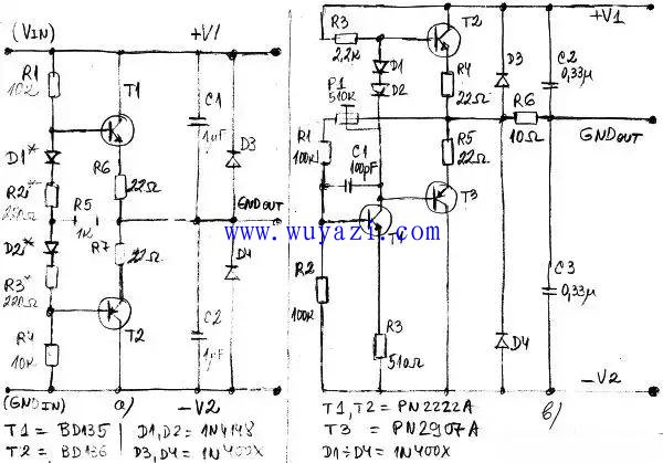 Figure 4: A voltage divider designed using a differential amplifier built into transistors.
Transistors T1 and T2 act as a differential amplifier, while T3 serves as an amplifier and driver for output transistors T4 and T5. Resistor R6 provides negative feedback to stabilize the output voltage. R7 and C2 are not required, but C1 is essential for frequency compensation.
The output voltages +V1 and -V2 are set using R1, R2, and P1. Diodes D1, D2, and D3 are used for biasing and temperature compensation of the output transistors. The trimmer P2 allows adjustment of the quiescent current of the output transistors, typically ranging from 1mA to 10mA depending on the load. Resistors R4 and R5 provide local negative feedback and offer some protection to T4 and T5.
Figure 4: A voltage divider designed using a differential amplifier built into transistors.
Transistors T1 and T2 act as a differential amplifier, while T3 serves as an amplifier and driver for output transistors T4 and T5. Resistor R6 provides negative feedback to stabilize the output voltage. R7 and C2 are not required, but C1 is essential for frequency compensation.
The output voltages +V1 and -V2 are set using R1, R2, and P1. Diodes D1, D2, and D3 are used for biasing and temperature compensation of the output transistors. The trimmer P2 allows adjustment of the quiescent current of the output transistors, typically ranging from 1mA to 10mA depending on the load. Resistors R4 and R5 provide local negative feedback and offer some protection to T4 and T5.