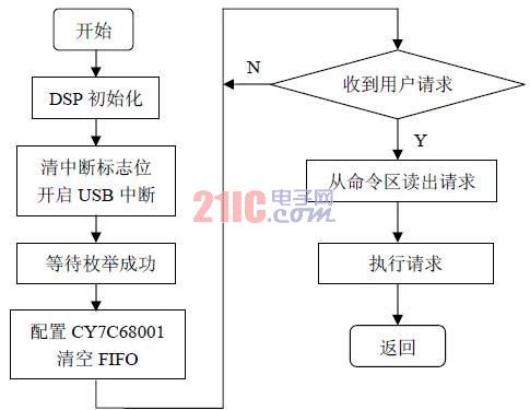
The development of digital signal processors is also changing with each passing day. Not only is the instruction speed faster and faster, but its power consumption is also getting lower and lower. Many instruments or inspection devices apply DSPs to systems that have a large amount of data and need to transmit data in real time. The nuclear signal data acquisition system is no exception. The DSP can process the collected signals in real time and send the processed data to the host computer for further processing. This article refers to the address: http:// Generally, the communication between the lower computer and the upper computer of the data acquisition system adopts the serial port mode, which is not only simple in protocol but also convenient in connection. However, the data transfer rate of this method is not high, and the USB bus interface has the advantages of convenience, fast support, plug and play, high-speed data communication, and the like, and is widely used in many fields. The USB bus interface can transmit up to 12Mbps under the USB1.1 protocol and up to 480Mbps under the USB2.0 protocol, which can fully meet the requirements of the current data acquisition and control system for the real-time data transmission rate. Therefore, in the design of this system, the communication method adopts USB (Universal Serial Bus) bus interface mode. The USB control chip uses Cypress's EZ-USB SX2 series CY7C68001 control chip, and the DSP uses TI's fixed-point DSP chip TMS320VC5502. 1. CY7C68001USB control chip introduction CY7C68001 is a high-speed USB chip developed by Cypress Corporation of the United States and supports the USB2.0 protocol. It integrates USB transceiver (physical layer), USB serial interface engine SIE (link layer, implements the underlying communication protocol), 4KB FIFO and voltage regulator, phase-locked loop; can work at full speed (12Mb/s) And high-speed (480Mb / s) two transmission modes, support 8-bit and 16-bit data bus mode, with synchronous and asynchronous FIFO interface. The CY7C68001 is used to connect to controllers such as DSPs, ASICs, and FPGAs to implement USB functions. It does not contain a microcontroller inside. At the same time, CY7C68001 provides 4 transmission modes (control transmission, interrupt transmission, bulk transmission and synchronous transmission), which can meet the requirements of users for various transmission methods. Since the control chip does not contain a microcontroller, the application layer protocol of USB should be implemented by DSP. The loading of USB firmware must be completed by DSP control CY7C68001. 2. Communication interface system hardware design The entire acquisition system includes sensor signal conditioning circuit, A/D conversion circuit, FIFO data buffer unit, DSP controller, FLASH program storage unit, CPLD logic control unit, and USB communication unit connected to the host computer. The hardware interface diagram of the USB unit that communicates with the PC is shown in the figure below. As can be seen from Figure 1, the communication part is mainly composed of CY7C68001 USB controller, CPLD logic unit, E2PROM, TMS320VC5502. Since the number of devices required for the entire system is large, the resulting logic control is complicated, and the I/O interface of the DSP is limited. Therefore, a CPLD logic control unit is added to the system to generate the logic state required in the circuit. . At the same time, the register function is also implemented in the CPLD. This part of the register is used to characterize various status information during USB communication, which is convenient for DSP query. The CY7C68001 USB controller and the TMS320VC5502 use an EMIF connection and configure the memory in the USB controller into the CE1 space. At the same time, the data and command exchange between TMS320VC5502 and CY7C68001 are completed by asynchronous read/write. The role of the E2PROM in the system is to complete the USB controller's description table bootstrapping. The CY7C68001 controller has two bootstrap modes: EEPROM and microcontroller. The system uses EEPROM. 3. Communication interface system software design 3.1 Host-side software design The function of the host software is mainly to complete the receiving, displaying and analyzing of the data uploaded by the lower computer. Due to the large amount of data collected by the signal, the bulk transmission method is adopted in the USB transmission mode. The design of the host software consists of three aspects: (1) USB driver design The function of the USB driver is mainly to implement USB discovery, configuration, shutdown, and data transfer interface control. The USB device driver is designed based on WDM (Windows driver model). WDM uses a layered driver model that is divided into higher-level USB device drivers and lower-level USB function layers. The USB function layer consists of two parts: a higher-level Universal Serial Bus Module (US-BD) and a lower-level Master Controller Driver Module (HCD). In the above USB layered module, the USB function layer is provided by the operating system and is responsible for managing communication between the USB device driver and the USB controller, loading and unloading the USB driver, establishing communication with the USB device universal endpoint to perform device configuration, Data and USB protocol framework and packaging format for two-way conversion tasks. (2) Install USB information file (.inf) This step is used to bind the driver to the Verdor ID (VID) and Product ID (PID) of a particular device. When the USB device is plugged into the computer, the computer detects that the device automatically issues a query request after it is inserted; the USB device responds to the request and sends the device's VID/PID. The computer completes the enumeration by loading the appropriate device driver based on these two IDs. (3) User application The user application is the core of the data acquisition system. Its main functions are: turning on or off the USB device, detecting the USB device, setting the USB data transmission pipeline, setting the A / D status and data acquisition port, collecting data from the USB interface in real time, displaying and analyze data. The entire application is written in Microsoft Visual C++, which enables A/D sampling and data display through control of the interface. BOOLEAN OpenDriver ( ); BOOLEAN CloseDriver ( ) ; PVO ID Sx2GetDeviceDesc ( ) ; PVO ID Sx2GetStringDesc ( int stringIndex) ; PVO ID Sx2GetConfigDesc ( ) ; BOOLEAN Sx2GetPipe Info ( PVO ID p Interface) ; BOOLEAN Sx2SendVendorReq ( PVO ID myRequest, char * buffer, int bufferSize, int * recnBytes) ; BOOLEAN Sx2GetPipe Info ( PVO ID p Interface) ; 3.2 DSP software program design Data transfer between the USB host and the device is done through an endpoint in the device. These endpoints are identified by endpoint numbers and input and output directions, and a fixed FIFO memory area is allocated for data transfers. The system configures the four endpoints of CY7C68001 as a bulk transfer type at initialization. Among them, FIFO2 and FIFO4 are output terminals for receiving data from the host computer; FIFO6 and FIFO8 are input terminals for storing data to be transmitted. Each FIFO is set to an asynchronous mode of operation. After the DSP is initialized, the USB external interrupt is opened, and the descriptor table is written to CY7C68001, waiting for its enumeration interrupt. After the enumeration is successful, the DSP performs other configuration on CY7C68001 and clears the FIFO, then waits for the host to send a user request and process accordingly. The software program flow chart is shown in Figure 2. Figure 2 DSP software programming flow chart The DSP software program design mainly includes the initialization of the DSP, the writing of the USB descriptor table and the configuration of other command registers, and the corresponding processing requested by the user. The initialization of the DSP is mainly to initialize the clock rate, configure the EMIF port, and configure the McBSP port. The USB descriptor table mainly completes the initial configuration inside the USB chip. The configuration of the command register is to complete the opening of the USB interrupt, the capacity of the endpoint data transmission, and the configuration of the direction. The user request is a user application that completes the corresponding data transfer according to the request sent by the user. 4 Conclusion The system uses the USB interface to complete the data transmission between the nuclear signal acquisition system and the host computer. The user program of the host computer displays the transmitted data and the waveform graph. The verification shows that the method is simple and reliable. Compared with the ordinary serial port, its speed has also been improved. The innovation of this paper is to use the traditional DSP signal acquisition system for the acquisition of nuclear signals, and to improve the serial port mode of communication with the host computer to USB mode. This plug-and-play interface is not only convenient and superior. The connection of the machine and the rate of transmission is increased.
Special Application safes are safes that are used in special scene and/or with special functions.
Details:
Solid steel construction;
Including data safes, medical safes and jewelry safes;
Electronic & mechanical panels are available;
Equipped with Mechanical Lock for the emergent opening of the safe
Special Application Biometric Fingerprint Treasure Safe,Intelligent Electronic Safe,Biometric Safes,Fingerprint Treasure Safe YONGFA INTELLIGENT TECHNOLOGY SECURITY CO., LTD. , http://www.yongfa-safe.com
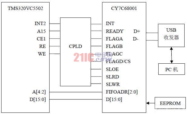
Figure 1 Hardware interface block diagram of data acquisition system and PC communication
Here are some of the application-related functions: