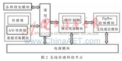
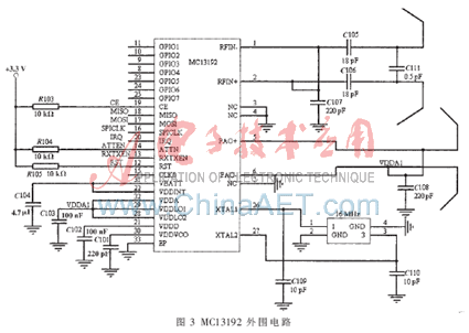
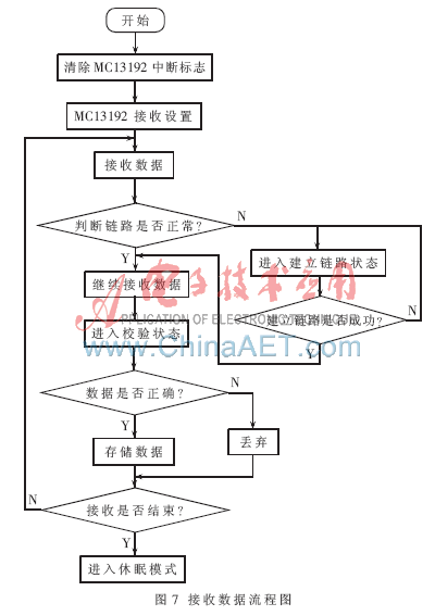
There are a large number of visually disabled people in countries around the world. How to improve their quality of life and solve the blind travel has become a common concern of all countries in the world. At present, the blind people still rely on the exploration sticks and simple touch to understand the world. There is a polarization of the market for blind people's appliances in China. The low-end life-study supplies and appliances are abundant, while the high-end products are extremely scarce. The blinding equipment molding products currently on the market are only at the initial level of obstacle alarms, and the practical functions are extremely limited. It is impossible to provide blind people with information sufficient to understand the surrounding environment, which is far from satisfying the needs of the blind. Many countries and scientific research institutions in the world are developing blind identification devices. For example, the blind binaural voice prompting system [1] uses ultrasonic to detect obstacles and road surface texture changes, and prompts through sound signals; Li Guangqiang uses DSP processor to develop a blind recognition and voice prompt system [2]; Chen Meizhen uses intelligent ranging and voice alarm method to design intelligent blind guide [3]; Xie Qiang converts image signals into FM audio signals, designs electronic blind aids [4]; He Jufang uses ultrasonic ranging, The method of transforming ultrasonic waves into sound waves is to design an electronic device that helps blind people to walk and identify obstacles [5]. This paper uses wireless sensor networks to design a new blind pedestrian guidance system. This article refers to the address: http:// 2 Wireless Sensor Network Node Design The wireless sensor network node is a miniaturized embedded system consisting of four parts: data acquisition module, microprocessor module, wireless communication module and power module, as shown in Figure 2. The data acquisition module is responsible for collecting information and converting the collected signals into digital signals for transmission to the microprocessor module; the microprocessor module is responsible for controlling the processing operations, routing protocols, power management, task management, etc. of the entire node. The ZigBee hardware platform used in this system can be divided into LPC2138 control module, MC13192 RF module, RS232 serial communication module, data acquisition module and power module. The LPC2138 is an embedded 32-bit ARM7 microcontroller with 512 KB of embedded high-speed flash memory and 32 KB of on-chip static RAM with two 8-channel 10-bit A/D converters and one D/A converter. External interrupts with 47 GPIOs and 9 edge or level triggers. Low Power RF Bidirectional Transceiver MC13192, IEEE 802.15.4 compliant, operates in the 2.4 GHz ISM band and provides 250 Kb/s data rate and 16 different channels with quadrature QPSK modulation and direct sequence spread spectrum coding Communicates with the MCU via a 4-wire serial interface. The A/D converter in the data acquisition module uses the AD7674 analog-to-digital converter with 18-bit high-precision resolution and a maximum conversion clock frequency of 800 MHz. 3 RF communication circuit design The MC13192 RF communication circuit includes the MC13192 support circuit and the antenna circuit, as shown in Figure 3. The MC13192 support circuit includes a power supply circuit, a filter circuit, and a crystal oscillator circuit. VBATT and VDDINT are power input pins. The normal operating voltage of the MC13192 is 2.0 to 3.6 V. The pin VBATT is connected in parallel with the pin VDDINT, and an external 4.7 μF F regulator capacitor is connected. Pins VDDA, VDDLO1, and VDDLO2 are connected in parallel, and a 100 nF filter capacitor is connected externally. The output voltage of the three pins is a rectified analog voltage. The pin VDDD output voltage is an internally rectified digital voltage. VDDVCO supplies power to the VCO circuit and is externally connected to a 220 pF capacitor. The XTAL1 and XTAL2 are externally connected to a 16 MHz crystal dedicated to a 2.4 GHz RF circuit with a bypass capacitor of 10 pF. The antenna of the MC13192 RF circuit uses a PCB type antenna. This type of antenna is suitable for use in a hardware platform of a wireless sensor network. RFIN- and RFIN+ are receive channels, and two 18 pF capacitors filter out high frequency interference signals. PAO- and PAO+ are transmit channels. These two pins are connected to VDDA to provide the necessary energy for the transmit channel. 4 Ultrasonic detection circuit design The principle of ultrasonic ranging is: the ultrasonic transmitting probe emits ultrasonic pulses, and the ultrasonic waves are transmitted from the measured object after being transmitted through the medium (air), and are received by the receiving probe. Based on the velocity v of the ultrasonic wave in the air, the time t from the transmission to the reception of the ultrasonic pulse is measured, and the distance L from the probe to the surface of the object can be calculated: 5 System software design system software part mainly includes main program processing module, initialization module, establishment of communication link module, communication service module and so on. The communication service module includes a data processing module, a package sending module, and an interrupt receiving module. The main program processing module is used to call other modules to complete the functions of the system. The initialization module is used to initialize the serial port of the microprocessor and set the parameters of the ZigBee module, including the setting of various internal registers and the setting of working mode (such as baud rate). A communication link module is established to establish a data link between nodes. The data processing module is used to receive and process data sent by the wireless sensor node. The packet sending module transmits the packet byte by byte by using the serial port interrupt when the information is packaged and sent. The interrupt receiving module is configured to receive data sent by the serial port, perform verification after the packet is received, and determine whether to discard the frame according to the verification result. The main program flow chart is shown in Figure 5. Radio frequency communication MC13192 module transmission data flow chart shown in Figure 6, the receiving data flow chart shown in Figure 7. The system uses GPS to measure the position of the blind person, uses ultrasonic to measure the distance, uses the CCD camera to capture the image of the object, uses the ZigBee wireless sensor network to transmit data, and collects the information to the blind voice prompt after computer processing. The design involves multiple interdisciplinary fields such as wireless communication and wireless technology, network technology, image transmission and processing technology, voice signal processing technology and computer technology. This system is a new attempt in the design of blind identification and guidance system. It can bring convenience to the life of the blind. The research and development of the system has very important economic and social benefits.
Internally Installed Digital LED Strip puts main part of the driver IC is integrated into the commonly used 5050RGB patch lamp bead.
reducing external components, reducing the volume and reducing the production cost.
Control circuit and RGB chip is integrated into a 5050 packaged component to form a complete external control pixel.
The three primary colors of each pixel can achieve 256 levels of brightness display, serial cascade interface,
and can receive and decode data through signal lines. The color of the light is highly consistent and cost-effective.
Generally used for LED full color luminous word string, LED full color module, LED full color soft light strip hard light strip,
Led Pixel Screen, LED shaped screen and so on. It is one of the most common ribbons on the market.
Internally Installed Digital Led Strip Digital LED Strip,5050Rgb LED,LED Strip Light Waterproof,Internally Installed Digital LED Strip SHEN ZHEN SEL LIGHTING CO.,LTD , http://www.sellighting.com
1 System Design The system uses GPS to measure the specific location of the blind person, uses ultrasonic to measure the distance between the blind person and the object, and uses the CCD camera to capture the image of the object. The information is transmitted to the computer through the ZigBee network. After the information is processed by the computer, the output is transmitted to the voice control board through the ZigBee network, and the voice is promptly presented to the blind person after the voice synthesis processing. The system not only helps the blind to determine the position of the direction and obstacles, but also identifies the type of obstacles, helps the blind to locate themselves in the designated community, and indicates the general direction of the destination. At the same time, the system can help blind people identify the surrounding objects and provide convenience for the blind daily life. The system uses the ZigBee network for wireless signal transmission. The schematic diagram is shown in Figure 1. ZigBee network nodes include common nodes, sink nodes, and gateway nodes. The ordinary node completes data acquisition through the sensor, the sink node performs multi-hop relay transmission, and the gateway node transmits the collected information to the PC through RS485 serial communication. Common nodes of the system include GPS measurement position, ultrasonic ranging, image acquisition and voice prompt module. A single ZigBee network node can cover 10 m indoors and 30 m to 75 m outdoors. The sink node can extend the ZigBee network coverage by multi-hop relaying the signal. 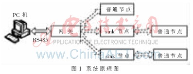

The circuit function module of the ultrasonic ranging system mainly includes three parts: a transmitting circuit, a receiving circuit and a micro processing circuit, as shown in FIG. 4 . The ultrasonic signal is generated by oscillation of the 555 time base circuit. The ultrasonic probe uses the transmitting sensor T40-10 and the receiving sensor R40-10. The center frequency of the probe is 40 kHz, the transmitted sound pressure is greater than 107 dB, and the receiving sensitivity is greater than -74 dB/V/μBar. 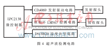

references
[1] KUC R. Binaural sonic electronic aid provids vibrotactile cues for landmark, reflector motion and surface texture classification [J]. IEEE Trans. on Biomedical Engineering, 2002, 49(10): 1173-1180.
[2] Li Guangqiang. Research and design of DSP-based blind target recognition system [D]. Xi'an: Northwestern Polytechnical University, 2006.
[3] Chen Meizhen, Yin Hao, Li Piao. Design and implementation of intelligent blind identification device[J]. Electronic Technology Application, 2006, 32(10): 4-6.
[4] Xie Qiang. Electronic blind aid. China: No.CN2650066Y[P].2004,10.
[5] He Jufang, Pan Guohua, He Junfeng. Electronic device for helping blind people to walk and identify obstacles. China: No.CN2843397Y[P].2006,12.
The advantage is that the circuit is integrated into the led bead, the external circuit can be omitted, and reduce the circuit design,