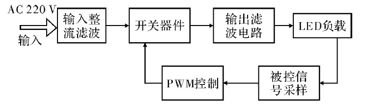
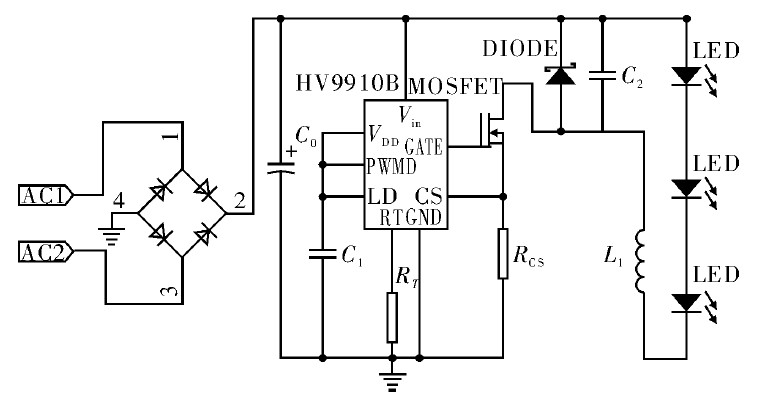
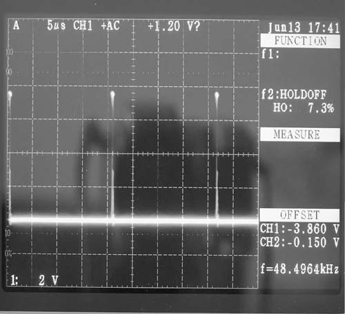
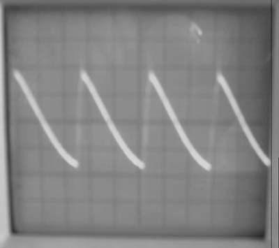
Abstract: Based on the analysis of LED electrical characteristics, according to its working characteristics, a high-efficiency white LED driver circuit with HV9910B as the core of the mains supply PWM mode is designed. Through the theoretical calculation and experimental measurement, the working frequency of the circuit is determined. The test results show that the driving circuit has a wide operating voltage range and constant current output, and the conversion efficiency exceeds 85%. With the rapid development of LED. Nowadays, the traditional light source of white LED light source has the advantages of long life, solid lighting, damage, high luminous efficiency, mercury-free environmental protection, earthquake resistance, etc. It will become the third generation light source in the future and will bring another revolution in the field of lighting. The use of LEDs in the field of illumination requires a driver power supply suitable for LEDs. In this paper, a high-power driver circuit for white LEDs is designed using PWM switch control. 1 LED electrical characteristics and drive requirements 1. 1 Electrical characteristics of LED The I-V characteristics of the white LEDs are similar to those of the conventional diodes, except that the turn-on voltage is different, and the LED turn-on voltage of the different materials is generally between 1.5 and 3. 0 V. When in the forward working area, the operating current IF is exponentially related to the applied voltage: Where, I S is the reverse saturation current; V F is the applied voltage across the diode; q is the electron charge; k is the Boltzmann constant; T is the thermodynamic temperature. The DC current that the LED can work stably for a long time is called the rated operating current. At this time, the LED voltage drop is called the rated voltage. 1 W white LED with a rated operating current of 350 mA and a rated voltage of 3.3 V. The maximum value of the product of the forward voltage and the current flowing through the LED is allowed to be its ultimate power consumption. When the actual power consumption exceeds this value, the LED's light-emitting characteristics become worse, which may cause structural damage to the LED. 1. 2 LED driver requirements According to the I-V characteristics of the LED, when the voltage applied across the LED fluctuates slightly, it will cause a drastic change in current. At this time, it is easy to make the current too large, and the input power exceeds its limit power consumption, thus making the LED unrecoverable. Damage. When the working current value of the LED is different, the luminous intensity is also different. If constant voltage driving is used, the LED array should be connected in parallel, but due to the parameter error between the individual LEDs, the current of each branch will be different, resulting in an array. The luminous intensity is not uniform, so the driving circuit of the LED generally selects the constant current driving mode, and the corresponding LED array is also connected in series. The driving current is generally set to 70% ~ 85% of the rated current of the LED to protect the LED and prolong the service life. The purpose is also to make the luminous intensity of each LED uniform. In the LED driver circuit design, the following basic indicators need to be considered: (1) Improve the conversion efficiency of the driver circuit and reduce the power consumption in the circuit.    (2) Improve the reliability of the circuit, withstand high voltage, and have overcurrent detection function.    (3) The circuit is as compact as possible, with a small circuit size and low manufacturing cost. 2 PWM mode switching circuit design 2. 1 PWM principle PWM is pulse width modulation, which uses pulse to control the switching time of the switching circuit to control the average voltage or current output from the circuit to achieve the output power of the control circuit. The basic working principle of PWM switching regulator or constant current is that under the condition of input voltage, system parameters and external load change, the control circuit performs closed-loop feedback through the difference between the controlled signal and the reference signal at a fixed operating frequency to adjust the main The pulse width of the circuit switching device is turned on, so that the output voltage or current of the switching power supply is stable. Since the power consumption of the control device is small and the circuit operating in the switching state is high, the power efficiency can generally be 80% to 90%. This type of circuit has perfect protection measures and is a highly reliable power supply. The PWM switching circuit consists of four parts, namely input rectification filtering, PWM control, switching device and output filtering. The LED driver circuit block diagram based on the PWM mode switching circuit design is shown in Figure 1. Figure 1 LED drive circuit block diagram of PWM mode switch circuit design Most of the common PWM switch control signal generation parts are integrated, and the design of the PWM switching power supply is more streamlined. The following describes the typical PWM mode switch drive circuit designed for high-power LEDs using the chip HV9910B. 2. 2 circuit design The HV9910B is a versatile LED driver controller that is adaptable to internationally powered mains, battery or solar, and accepts a wide range of input voltages. The output constant current drive current range is extremely wide, from tens of mA to more than 1 A. Drives built with the HV9910B use fewer components, simpler circuits, and lower production costs. The LED constant current drive circuit designed by HV9910B is shown in Figure 2. The input is AC 220 V mains, and the load is 10 LEDs in series with 1 W. Figure 2 LED driver circuit based on chip HV9910B control The input stage of the circuit consists of a full-wave rectifier bridge and a filter capacitor to complete the rectification and filtering of the AC power. The control stage is built by the HV9910B chip. The voltage filtered by the input stage is input to the Vin of the chip. As the input voltage VI of the circuit, the peak value is 310 V, and the average value is 190 V. The LD and PWMD terminals are connected to the GND terminal through the capacitor. To maintain the on-chip voltage of the corresponding pin. The square wave pulse signal with a certain frequency output from the GATE terminal is used as the switch signal to control the switch tube. The frequency is set by the resistor connected to the RT terminal, and the pulse width is controlled by the LED current signal fed back by the CS terminal sampling resistor RCS. Inductor L1 plays a vital role in the circuit, providing filtering and energy storage and freewheeling power to the drive circuit to maintain the current balance in the load, and the recovery diode completes the construction of the freewheeling path. During the half cycle of the switching signal being turned on, the pre-filtered potential is directly supplied to the LED load, and the L1 is charged; in the half cycle of the switching signal being turned off, the energy-rich L1 is used to supply the circuit composed of the fast recovery diode and the LED. Achieve continuous driving of the LED in one cycle. 2. 2. 1 circuit parameter calculation and device selection The reference chip's manual and specific circuit requirements can determine the peripheral device parameters of the chip. First, the operating frequency of the circuit must be determined. A resistor with a resistance value of 226 kΩ ~ 1 MΩ on the RT pin sets the frequency of the switching signal output from the GATE pin. The choice of this frequency is related to the inductance L value and the performance of the switching tube. Generally, under the mains supply condition, the frequency is selected from 25 to 150 kHz. When the frequency is too high, the required inductance value is small, but the requirements on the switch tube are very high. At this time, the power consumption of the switch tube is much larger than that at the low frequency operation. In the test, the switching frequency was set to 100 kHz, and the MOSFET generates a large amount of heat without heat dissipation, which is extremely easy to burn. When the frequency is set to 26 kHz, the calculated inductance is very large. In the working state, the inductor consumes too much energy and is not suitable for the high efficiency operation of the circuit, so the switching operating frequency is 50 kHz. The driving current of the LED is set to 0.35 A. According to the calculation formula provided in the chip manual, the RT value is 478 kΩ. 470 kΩ resistor can be used as R T and the sampling resistor R CS = 0. 62 Ω. The value of the inductance L1 is related to the ripple value of the LED current. Generally, the ripple coefficient is limited to 0.3. The calculation formula of the inductance value is: The circuit drives 10 LEDs with a VLEDS of 33 V. Vin is the full-wave rectified and filtered peak voltage with a value of 310 V. The ILED and fs are the same as before, and the substitution (2) is calculated as L1 = 5 6 mH, the inductor used in the circuit is 6. 8 mH. The MOSFET has a high-performance IRF840 with a maximum withstand voltage of 500 V, a maximum drain current of 5 A, and an on-resistance of 0.6 Ω. The diode is selected as the fast recovery diode BYV26B, the reverse withstand voltage V D = 500 V, the forward average current is 1 A, the forward voltage drop is 1. 2 V. The capacitor C2 is used as the output filter circuit to achieve voltage filtering, C2 is 4. 7 For the capacitor of ~33 μF, the filter capacitor C0 of the previous stage is selected to be a polar capacitor of 4. 7 ~ 33 μF, and the capacitor C1 is a capacitor of 2. 2 μF. The full-wave rectifier bridge requires high withstand voltage and large overcurrent. The DB206S is selected in the circuit, which can withstand pulse high voltage of 800 V and surge current of 2 A to meet the circuit design requirements. 2. 2. 2 Circuit efficiency theoretical calculation reference The main loss in the whole circuit is generated by the power MOS transistor, the sampling resistor, the inductor L1 connected to the load LED, the fast diode and the chip HV9910B [7]. According to the relevant formula provided by the literature [7] and the original parameters of the specific model, it can be calculated. Obtain the overall power consumption of the circuit P LOSS = P MOS + P DIODE + P INDUCTOR + P IC + P RS = 0. 032 +0. 389 + 0. 613 + 0. 31 + 0. 008 = 1. 352 W. The output power of the circuit is P O = 33 × 0. 35 = 11. 6 W, the overall conversion efficiency of the circuit η = 11. 6 / ( 1. 35 + 11. 6) × 100% = 89. 57%. From the calculation results of the efficiency theory, the design circuit has excellent performance. 3 circuit test The circuit design of the designed PWM switch drive circuit is carried out, and the working state of the physical circuit is tested by using a digital voltmeter, an AC power meter, an oscilloscope and the like. The voltage waveforms of the two key points in the circuit are tested under normal circuit operation. Figure 3 shows the PWM switch control signal waveform applied to the gate of the switching device. The period is 14 μs, the amplitude is 8 V, and the duty ratio is 8.3%. There is a certain gap between the period and the preset value. This is mainly the resistance of the RT. The frequency setting deviation caused by the value error. Figure 4 shows the waveform of the current in the LED load. The measurement process is to measure the voltage waveform across the 0. 5 Ω resistor in the LED load loop, and use the linear characteristics of the resistor to reflect the current characteristics. From the waveform, the current is periodically changed according to the sawtooth waveform, and the peak-to-peak value is 40 mV. The current ripple is 80 mA, and the average output current is 350 mA. The ripple coefficient is calculated to be 22.9%. Figure 3 PWM switch control signal Figure 4 Current waveform in the LED load The input power of the circuit is actually measured to be 9. 9 W, and the load power consumption Pout is 8.7 W. The conversion efficiency of the circuit is 87.8%, which is similar to the theoretical calculation of the circuit efficiency. After measuring the key point waveform of the circuit and measuring the power of the circuit, the circuit is operated at a frequency of 71 kHz, the working state is stable, the output power is large, and the efficiency is high. However, the output ripple coefficient of the circuit is too high, so that the illuminance of the LED in safe operation will not reach its optimal value, and further improvement and improvement of the circuit output filtering part is needed. 4 Conclusion Through analysis to understand the LED luminescence performance and electrical characteristics, the drive requirements for driving the LED array in series using a constant current source are obtained. Based on the principle of PWM mode switching circuit, a typical PWM mode switching circuit based on HV9910B chip is designed. The optimal working frequency is determined by experimental measurement, and the illumination driving of white light high power LED is well completed. Through theoretical calculations and actual measurements, it is found that the switching LED driving power supply has superior circuit conversion efficiency, wide operating voltage range, constant current output and conversion efficiency exceeding 85%. However, to drive the white LED more safely for daylighting, it is necessary to perform a more excellent filtering process on the output of the switching circuit, so that the output ripple of the circuit is smaller and the current is more stable.
Coupletech
Co., Ltd. Supply CW Laser models for medical instruments and scientific
research, consists of UV laser GN-355, Low noise blue laser GL-473, Low noise green laser DL-532nm, Signal mode
green laser CS-532, Sodium Yellow Laser GL-556, Light yellow laser GL-561,
Orange yellow laser GL-593 and Infrared laser GL-1064, and these laser models cover
a wide range of wavelengths: 355nm, 473nm, 532nm, 556nm, 561nm, 593nm, 1064nm,
and son. The application of CW laser models is for Fluorescence stimulated for
biological medical instruments, Interferometry, laser hologragh, flow
cytometry, physical instruments, scientific research and so on. The average output power is
10 mW ~ 2000 mW, beam diameter at the aperture is ~ 1.5mm. Besides, single mode fiber coupled or customized is optional.
Diode Pumped CW,Diode Pumped Solid State Laser,Solid State Laser Diode Coupletech Co., Ltd. , https://www.coupletech.com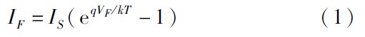


4 times
Window._bd_share_config = { "common": { "bdSnsKey": {}, "bdText": "", "bdMini": "2", "bdMiniList": false, "bdPic": "", "bdStyle": " 0", "bdSize": "24" }, "share": {}, "image": { "viewList": ["qzone", "tsina", "tqq", "renren", "weixin"], "viewText": "Share to:", "viewSize": "16" }, "selectShare": { "bdContainerClass": null, "bdSelectMiniList": ["qzone", "tsina", "tqq", "renren" , "weixin"] } }; with (document) 0[(getElementsByTagName('head')[0] || body).appendChild(createElement('script')).src = 'http://bdimg.share. Baidu.com/static/api/js/share.js?v=89860593.js?cdnversion=' + ~(-new Date() / 36e5)];