Wonke Electric CO.,Ltd. , https://www.wkdq-electric.com
Since the introduction of integrated circuits, temperature sensors have become an integral part of IC design. Engineers have long sought to minimize the impact of temperature on chip performance. Integrated temperature sensors can effectively address most temperature sensing challenges within a wide range of -55°C to 200°C. The latest generation of these sensors achieves ±0.4°C accuracy in a compact 0.76mm² package, making them ideal for space-constrained applications.
From the beginning of the IC design era, temperature sensors have naturally become part of device architecture. Designers have continuously worked to reduce the influence of temperature on system performance. However, some engineers took a different approach: instead of trying to eliminate the effects of temperature, they explored ways to use it. This led to the development of temperature sensors that actively exploit the behavior of pn junctions in active circuits. As digital functions became more integrated into chips, designers became even more innovative, leading to the creation of advanced current-based temperature sensor ICs.
The integrated temperature sensor is capable of solving most temperature sensing issues within the range of -55°C to 200°C. Its design allows for high accuracy and reliability, even in extreme conditions.
The input to a temperature sensor IC is the ambient temperature. When the surrounding temperature changes, it affects the behavior of internal transistors, as shown in Figure 1.
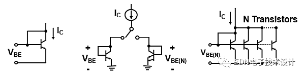
**Figure 1:** This conceptual circuit demonstrates how a matched transistor detects temperature.
The temperature sensing design eliminates the effects of transistor saturation current (IS) through clever configuration and calculation. A constant current source (IC) and a switch between the transistor and an equivalent array are used to control this current.
In Figure 1, the difference between VBE and VBE(N) corresponds directly to temperature changes. Equation (1) represents the base-emitter voltage of a transistor:
$$
V_{BE} = \frac{kT}{q} \ln\left(\frac{I_C}{I_S}\right)
$$
Where:
- $ k $ is the Boltzmann constant, equal to $ 1.38 \times 10^{-23} $ J/K.
- $ q $ is the elementary charge, equal to $ 1.6021765 \times 10^{-19} $ C.
- $ T $ is the temperature in Kelvin.
Equation (2) shows the base-emitter voltage of multiple parallel transistors:
$$
V_{BE(N)} = \frac{kT}{q} \ln\left(\frac{I_C}{N I_S}\right)
$$
If the current source is switched between two transistors, the difference between their base-emitter voltages is given by Equation (3):
$$
\Delta V_{BE} = \frac{kT}{q} \ln(N)
$$
This simplifies to a constant value of $ 86.25 \times 10^{-6} \times \ln(N) $, which allows for accurate temperature measurement at the IC level. With these improvements, modern IC temperature sensors achieve remarkable accuracy, up to ±0.4°C.
**Output**
Once the temperature is accurately measured, it must be presented to the outside world. There are two main methods: analog voltage or digital output.
Analog voltage outputs are straightforward and easy to interpret. With the right sensor, you can capture an analog signal, convert it to a digital format, or feed it back into the circuit for further processing.
Digital outputs offer more flexibility, with various communication protocols such as 1-wire, 2-wire, or 3-wire interfaces. For example, 1-wire outputs can provide PWM signals or threshold switches, useful in fan control systems. 2-wire outputs typically use I2C or SMBus, while 3-wire outputs often support SPI.
**Wafer-Level Packaging of Temperature Sensor Devices**
Every product goes through a development process, and temperature sensors are no exception. The next major advancement comes in the form of wafer-level packaging (WLP). This technology allows for ultra-small packages that significantly reduce the overall size of the sensor.
WLP was first developed by Sandia National Laboratories and Fujitsu in 1998. The package is fabricated at the wafer level before dicing, and then assembled using standard surface mount technology (SMT).
This packaging method results in a very small form factor and low thermal resistance. The size of these sensors is so small that they can fit in the space of a standard 0.1μF capacitor in a 0603 package, as shown in Figure 2.
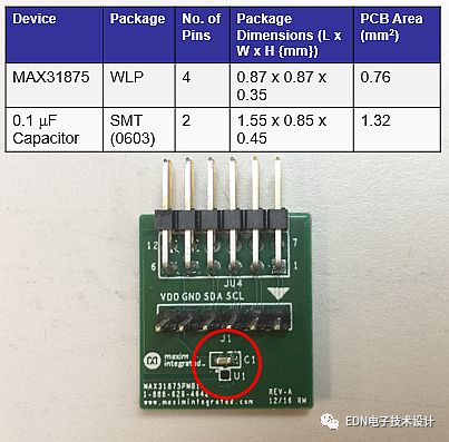
**Figure 2:** The WLP temperature sensor is much smaller than a typical 0.1μF SMT capacitor.
**Placement on PCB**
Thanks to its tiny size, the new package allows for flexible placement on a PCB, similar to how salt and pepper are sprinkled on a dinner plate. The latest temperature sensors achieve ±0.4°C accuracy in a package that occupies just 0.76mm² of board space, making them ideal for modern, compact electronic designs.