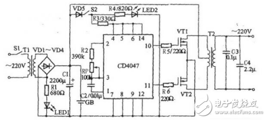
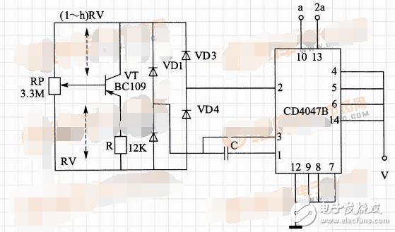
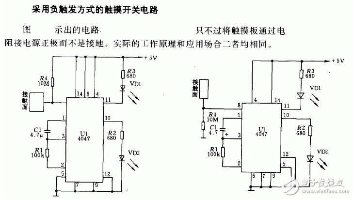
1. Inverter Power Supply Circuit Using CD4047 Multivibrator This is a low-power inverter power supply that delivers 30 W of output power, making it suitable for powering small devices such as low-power bulbs, energy-saving lamps, and black-and-white televisions during power outages. The circuit consists of three main sections: a charging circuit, a multivibrator oscillator, and a power output stage, as illustrated in Figure 4-7. The charging circuit includes a power switch S1, a step-down transformer T1, four rectifier diodes (VD1 to VD4), a resistor R1, a charging indicator LED VL1, and a filter capacitor C1. When the switch S1 is turned on, the AC voltage from the mains is first stepped down to 12 V by T1, then rectified by the diodes and filtered by C1 to charge the battery GB. The LED VL1 lights up to indicate that the charging process is active. The multivibrator circuit is built around the CD4047 IC, along with resistors R2 to R4, a potentiometer RP, a capacitor C2, a diode VD5, a switch S2, and an inverter operation indicator LED VL2. When the inverter is activated, S1 is turned off, and the +12 V DC voltage is supplied to the transistors VF1 and VF2 through the primary winding of the step-up transformer T2. After switching on S2, the +12 V also powers the CD4047 IC via VD5 and R3, lighting up VL2 to show that the inverter is operating. The CD4047 generates two 50 Hz square wave signals at its output pins 10 and 11, which are out of phase. These signals drive the high-power FETs VF1 and VF2, which alternately switch on and off, producing an alternating current across the secondary winding of T2. This results in an output of approximately 220 V AC. To increase the inverter’s output power, you can use a larger battery, a more powerful transformer, or connect multiple FETs in parallel. Additionally, adjusting the resistance of the potentiometer RP ensures that the multivibrator operates at exactly 50 Hz, matching the standard AC frequency. Figure 4-7: Inverter Power Supply Circuit Using CD4047 Multivibrator 2. Linear Oscillator Circuit Using CD4047B as the Core This circuit functions as a linear CMOS oscillator, primarily based on the CD4047B integrated circuit. It is designed to generate stable oscillation signals with adjustable frequency. The circuit diagram shows a configuration where a potentiometer RP and a transistor VT form a control network that adjusts the relationship between frequency and linearity. By varying the resistance of RP, the oscillation frequency of the CD4047B can be adjusted over a range of 1:100. The emitter resistance of the transistor VT and the variable base voltage work together to regulate the collector current, ensuring stable operation. The diodes VD1 to VD4 form a bridge that ensures symmetrical operation during both positive and negative half-cycles of the signal, improving the quality of the output waveform. As shown in the figure, this is a linear oscillator circuit based on the monostable trigger/unstable multivibrator CD4047B. It is commonly used in applications requiring precise and stable oscillation, such as in communication systems or signal generation. Linear Oscillator Circuit 3. Touch Switch Circuit Using CD4047 Pin Header section Pin Header section HuiZhou Antenk Electronics Co., LTD , https://www.atkconn.com