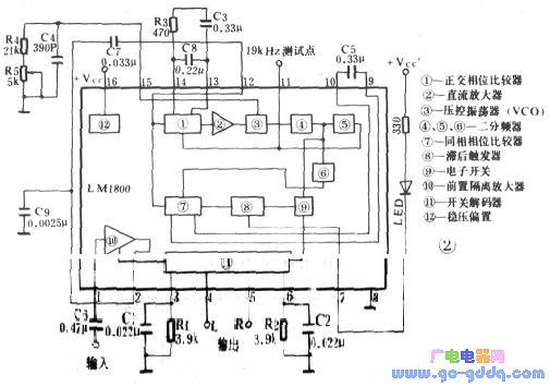
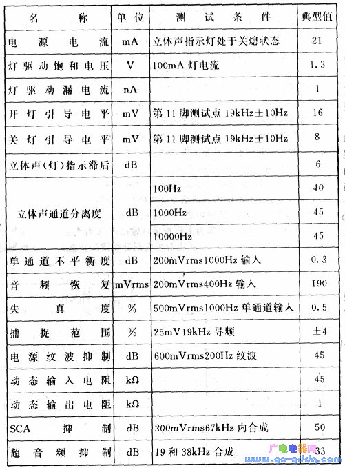
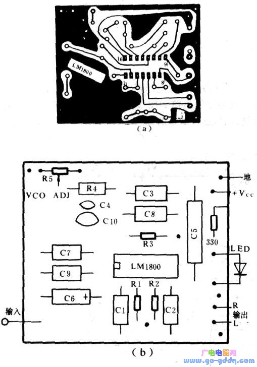
The LM1800 is a phase-locked loop FM stereo decoder monolithic integrated circuit introduced by National Semiconductor. This integrated circuit employs advanced phase-locking techniques to minimize the phase shift Ï between the 38 kHz switching signal reproduced within the integrated block and the 38 kHz subcarrier signal in the original primary and secondary channel composite signals, and maintains strict synchronization. It has high resolution and stable superior performance. At the same time, it also saves the complicated LC tuning state road peripheral components, which makes the circuit simplified and easy to debug. The IC is widely used in high- and mid-range FM stereo radios, stereo tuners and stereo systems. 1. Block diagram and internal circuit The internal circuit schematic of the LM1800 is shown below. It uses new circuits and new components such as dual differential analog multipliers and multi-pole transistors, and has a high degree of integration. The figure below is a block diagram of its internal circuit structure. The stereo composite signal obtained by frequency modulation and frequency discrimination is injected from the first leg of the LM1800, and is preamplified by the IC. The amplifier is divided into two outputs: one is directly sent to the input of the stereo decoder composed of the double differential analog multiplier in 1C. For the composite signal decoded by the stereo switch; the second pin of the other routing IC is taken out to the 12th pin of the TC via the external coupling capacitor C7 (0.033μF). The two output signals are respectively added to the 1C internal quadrature phase comparator and the in-phase phase comparator for phase comparison. The quadrature phase discrimination channel is composed of a quadrature phase comparator, a DC amplifier, a 76 kHz voltage controlled oscillator, and three two-divider circuits. It is divided twice and shifted by 90. The obtained 19 kHz orthogonal square wave signal is sent to the quadrature phase comparator for orthogonal phase discrimination with the 19 kHz pilot signal in the stereo composite signal injected by the 12th pin. When the phase difference between the two is not orthogonal or the frequencies of the two are not the same, the quadrature phase comparator has an (error) signal output. This signal is smoothed by an external (lC 1413) RC low-pass filter and sent to a DC amplifier for DC amplification. The amplified corresponding (error) signal is sent to the voltage-controlled oscillator to control the voltage-controlled oscillator frequency. , causing its phase and frequency to change in the direction of decreasing error. Through the multiple loops of the above-mentioned phase-locked loop feedback control process, the two sides achieve the quadrature phase locking and the frequency are completely consistent, thereby ensuring strict synchronization of the obtained 38 kHz subcarrier signal in the lC with the original 38 kHz subcarrier signal of the broadcasting station. . The in-phase phase discrimination channel consists of an in-phase phase comparator, a hysteresis trigger (stereo indicator driver), and an electronic switching circuit. The 19 kHz in-phase square wave signal obtained by two frequency divisions is sent to the in-phase phase comparator to perform in-phase phase discrimination with the 19 kHz pilot signal in the stereo composite signal injected by the 12th pin. The in-phase phase comparator then outputs a corresponding signal proportional to the amplitude of the pilot signal. When the receiver operates in mono or the received stereo signal is weak, the output of the in-phase phase comparator is difficult to put the hysteresis trigger and the electronic switch into operation, and the stereo decoder operates in the mono state. The output of the non-inverting phase comparator drives the hysteresis trigger and the electronic switch into the working area only when the receiver is operating in stereo reception and has sufficient signal strength. At the same time, the 38kHz switching signal is added to the decoder in 1C, and the stereo composite signal obtained by the south isolation preamplification is also injected into the decoder, so that the output of the left and right channel stereo audio signals after the switch decoding is obtained at the 4th and 5th pins of the IC. At the same time, the 1C pin 7 external stereo indicator is also driven to illuminate to reflect the presence and strength of the 19 kHz pilot signal in the broadcast station signal. 2. Typical application circuit of performance parameters and application circuit LM1800 is shown in Figure 2. The stereo composite signal obtained by the receiver's high frequency, intermediate frequency amplification and frequency modulation is injected into the IC pin 1 by stereo blocking coupling capacitor C6 (0.47μF) for stereo decoding. The pilot signal amplified by the IC is sent from the IC Z pin via the external coupling capacitor C7 (0.033μF) to the 12th pin of the lC as the input signal of the phase comparator. R3 (470Ω) and C3 (0.33μF) connected to pins 13 and 14 of the IC form a low-pass filter for the phase-locked loop. Its bandwidth and the size of the external pilot signal will determine the capture range of the entire phase-locked loop. . R4 (21kΩ), R5 (5kΩ potentiometer) and C4 (390pF) connected between pin 15 of LC and ground are external RC charging and discharging networks of voltage controlled oscillator (vco). Adjusting the trimmer potentiometer R5 adjusts the natural oscillation frequency of the vc0 circuit. The left and right channel signals decoded by the LM1800 are output by the IC pins 4 and 5. The circuit inside lC adopts a symmetrical emitter-transfer circuit structure, so it has a strong load capacity. lC 3rd and 6th feet are connected to R1, R2 (3.9kΩ) and Cl, C2 (0.022μF) for the ic inner cane sub-Jr parent decoder nickname to the H: level collector load network. The main electrical performance parameters of the LM1800 are listed in the table. It is easier to debug. The phase-locked loop is first adjusted to obtain a 38 kHz regenerative sub-carrier switching signal that is fully synchronized with the pilot signal in the original stereo composite signal. Then connect the frequency counter to pin 11 of lC to detect the frequency of the 19 kHz signal in the IC. The combined signal is then injected by the stereo multiplex signal generator and the vc0 natural oscillator frequency adjustment potentiometer R5 is carefully adjusted until the frequency counter reads 19 kHz ± 10 Hz. When there is no manual adjustment of the test instrument, the degree of debugging can be judged according to the degree to which the stereo indicator of the external pin of the IC is driven to illuminate. Finally, the subsequent circuit of the stereo decoder (ie, the left and right channel symmetrical audio voltages, power amplifiers) can be used to obtain a satisfactory stereo reception decoding effect. The printed circuit board diagram of the typical application circuit of LM1800 is shown in the figure below, which is used for reference when designing and making. Fume Ultra Vape,Fume Ultra Disposable Vape,Fume Ultra Disposable 2500 Puffs,Fume Ultra 2500Puffs Vape Nanning Nuoxin Technology Co., LTD , https://www.nx-vapes.com