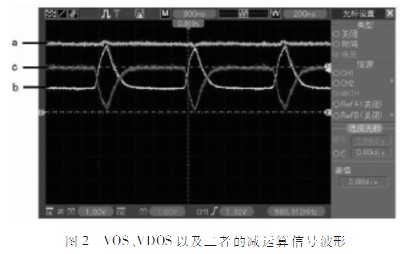
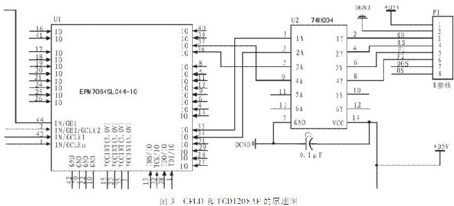
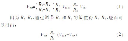
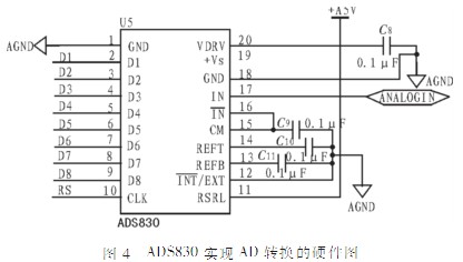
The core of the spectrophotometer is the spectral acquisition and processing system, which collects the spectral signals absorbed by the material through the photoelectric conversion device and displays them in real time through the display device. Conventional spectrophotometers usually use photocells to achieve this conversion. Because of the large size of photocells and the need for complex mechanical devices to project spectra onto photocells, traditional spectrophotometers are very bulky and expensive. Very expensive. The development of CCD technology has revolutionized the spectrophotometer. Due to the easy integration of CCD technology and fast acquisition speed, the spectrophotometer is gradually developing towards miniaturization and portability. The spectral acquisition system of the spectrophotometer proposed in this paper can be used to test the absorption intensity in the visible light band and the initial estimation of the absorption amount by using the coordination work of the CCD and the microprocessor component, thereby providing a reference for the material analysis. 1 CCD drive and noise processing technology research 1.1 CCD drive timing study The CCD is an ideal device for photoelectric conversion because of its low noise, high transfer efficiency, and fast spectral response, which uses alternating pulses to remove the optical signal stored therein and represent it as a voltage output. Due to the high transfer efficiency, its operating frequency is generally in the MHz standard. The CCD device used in this paper is the TCD1208AP linear array CCD device produced by Toshiba Corporation with the highest transfer frequency of 1 MHz. The TCD1208AP consists of 2,212 basic pixels, of which only 2,160 are available for spectral data conversion. Other pixels are used to control noise and fill data frames. The size of each pixel of TCD1208AP is 14μm & TImes; 14μm, so the dispersion capability of the dispersive device is not very high, and its high optical sensitivity and high operating frequency make its spectral acquisition very fast, reaching ns level. . By utilizing the property of the material to absorb monochromatic light, under the action of the dispersive device, light of different wavelengths is mapped to each pixel position on the CCD sensor, and each pixel position corresponds to the intensity of light of one wavelength. The relationship between the pixel and the wavelength can be calibrated by the microprocessor. The sensor collects optical signals of different wavelengths. The intensity of the optical signal is related to the time when the CCD is irradiated (the integration time of the CCD). Each image can be affected by changing the integration time. The amount of light intensity on the element. The normal operation of the TCD1208AP requires four drive pulses, namely the integral time control pulse SH, the optical signal transfer pulses φ1 and φ2 in the picture element, and the reset signal RS for clearing the residual charge in the CCD picture element. The timing diagram of the four-way drive pulse is shown in Figure 1. The RS generally operates at a speed of 1 MHz, the duty cycle of the pulse is 30%, the duty ratio of φ1, φ2 is 50%, and SH is the integral time control pulse of the CCD. In the case where the RS is 1 MHz, the period of SH is 452 ms, that is, the time of 2212 RS cycles. When starting work, φ1, φ2 must be at a high level before SH, so that the potential difference can be established immediately when SH arrives, so that the charge of the CCD is smoothly transferred out. 1.2 CCD noise processing technology The output signals of TCD1208AP are VOS and VDOS. VOS is the effective output signal doped with noise. The main component of noise is the reset noise caused by RS, and VDOS is the compensation output. The output signal of the CCD is doped with a DC level and an RS reset pulse, so the DC level (1.08 V shown) and RS (1 MHz reset pulse) pulses must be filtered out during analog to digital conversion. . The DC level filtering can be achieved by using VDOS compensation output, by adding and subtracting between VOS and VDOS. Figure 2 shows the signal diagram after filtering out the DC level. The signal c in the figure is the spectral absorption signal with reset noise without DC level. The effective spectral absorption signal after the reset pulse, the extent to which the substance absorbs light of different wavelengths is reflected in the magnitude of the signal. The cancellation of the reset noise is achieved by selecting the sampling points in the analog to digital. The subsequent signal processing process is performed by setting the sampling time in the effective spectral signal region and converting the voltage value of the video signal to a digital value at that time. The sampled pulse has two sources, one is by introducing an additional pulse source and realized by precise control; the other is realized by using the reset pulse RS of the CCD, and it is found that the pulse width region of the reset pulse RS of the CCD is located exactly The effective spectral signal region of the CCD, so the reset pulse can be used as the sampling pulse input of the analog to digital signal conversion section. 2 Key hardware circuit design in spectrum acquisition system The hardware circuit of the spectrum acquisition system is mainly used to realize the acquisition and conversion of the absorption spectrum of the material and the appropriate processing of the converted spectral data. Therefore, the stable and high-precision hardware circuit is the basis for the efficient and accurate operation of the spectrum acquisition system. 2.1 Research on CCD drive and CCD pre-processing circuit design The normal operation of the CCD requires the cooperation of an accurate clock. The TCD1208AP linear array CCD is selected as the photoelectric conversion device of this paper, which requires four clock pulses to drive: SH, φ1, φ2, RS. The four-way pulse has an amplitude of 5 V and is a standard TTL logic level. The driver design can be implemented using a microprocessor or a logic array such as an FPGA or CPLD. However, the clock accuracy of the microprocessor is relatively low compared to the logic array, and there is a problem that the phase is not synchronized. Therefore, the scheme designed in this paper is implemented by using CPLD. The chip is Altera's MAX7000 series EPM7064SIA4, and its IO port has 5 The output capability of the V level can be directly connected to the TCD1208AP without the need for other level conversion chips. The hardware connection diagram is shown in Figure 3. The CPLD uses a 10 MHz active crystal oscillator input. In order to improve the driving capability of the CPLD, the inverter 74HC04 is used to amplify the driving pulse of the CPLD output. Due to the inversion of the 74HC04, the driving pulse of the CPLD is high and low. The pulses that normally drive the CCD must be inverting. The clock of the CPLD input is 10 MHz, which is very frequency-efficient by the HLD hardware programming language and outputs a 1 MHz CCD reset pulse. Section 1.2 discusses the use of VOS and VDOS addition and subtraction to achieve spectrum The DC level is filtered out of the signal, and the hardware uses an operational amplifier to implement the process. This system uses AD company's AD8051 operational amplifier, its working bandwidth is up to 110MHz, the lower settling time makes it more capable of processing high frequency signals. According to the basic operational amplifier calculation rules, the output signal Vout is: Adjusting the value of R9 can change the output value of Vout. At this time, Vout is the spectral absorption signal of the substance without DC level. The processed material absorbs the spectral signal and enters the AD conversion module, where the reset pulse in the spectral signal can be filtered to obtain an effective spectral signal. The AD conversion chip used is BB's 8-bit analog-to-digital conversion chip, which has a sampling rate of 60 MHz and a high signal-to-noise ratio of 49.5 DB, making its conversion rate and accuracy meet the high-speed and high-precision of the spectrum acquisition system. Requirements. The ADS830 requires 4 clock cycles to complete the data sampling and digital signal output. When receiving the digital signal converted by the ADS830, it is necessary to control the timing of receiving the data so as to obtain the required data accurately. Figure 4 shows the conversion circuit for digitizing the spectral data using the ADS830. The ANALOGIN input is the spectral data without the DC level post-processed by the AD8051. Since the input voltage range of the ADS830 is 1.5 to 3.5 V, in order to make the spectral signal passing through the AD8051 in this range, it is necessary to adjust the value of R9. D1 ~ D8 is the converted spectral signal, which is sent to the microprocessor for subsequent processing.
Win 3 Cap Lamps are made of high intensity engineering plastic. With optimized construction structure, the lamps are explosion proof, impact proof, water proof, dust proof, flame proof. The high quality Cree LED has a lifespan of more than 30,000 hours and the phosphate technology battery more than 1000 cycles.
3 color options to be customized, pure white color, cool white color, warm color.
2 lighting models available, primary light and auxiliary light.
Mining Lights,Led Mining Light,Coal Mining Lights,Rechargeable Mining Cap Lamps ZHEJIANG HUACAI OPTIC-TECHNOLOGY CO LTD , https://www.win3safety.com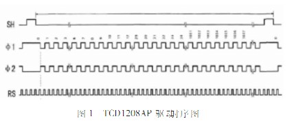
Trace substance composition and content analysis play an important role in scientific research, security inspection and other fields. At present, the common method of trace component analysis is to use a spectrophotometer. The principle is to use the absorption characteristics of light by a substance, measure its absorbance, estimate the composition of the substance by the position of the absorption peak, and estimate the content of the component by using the height of the peak. The traditional spectrophotometer is mainly used in the analysis and detection of substances, and its function is relatively simple. With the development of chip integration technology and the advancement of grating technology, the current spectrophotometer has undergone a revolutionary change in function, volume, and detection speed. For example, the use of a spectrophotometer to form a field soil monitoring network can detect the soil content of the soil in real time, so that agricultural producers can effectively improve the soil in a certain area to improve the yield.