introduction In DSP-based video processing systems, video capture methods can generally be divided into two categories: automatic video capture and DSP-based video capture. The former usually uses CPLD/FPGA to control the video decoding chip, and transmits data to the DSP through FIFO or dual-port RAM. The characteristic is that the data acquisition module runs independently, occupies less DSP resources, but the implementation is relatively complicated and the cost is high; the latter is usually controlled by DSP. The video decoding chip synchronizes various timings and reads the video data. The feature is that the implementation is relatively simple and the cost is reduced, but the control of the video decoding chip is complicated, and the DSP processing time is occupied. If the digital image sensor chip is directly connected to the DSP through appropriate logic circuits, the video control decoding chip, CPLD/FPGA, FIFO or dual-port RAM can be omitted, and the complexity of the system can be greatly reduced without increasing the DSP software overhead. Degree and cost, shortening the development cycle. Hardware system design System overall structure System block diagram shown in Figure 1. The DSP uses TI's C6000 series high-speed floating-point signal processor TMS320C6713, which has a peak processing speed of 1350 MFLOPS (million floating point per second). The external memory interface (EMIF) includes four CE spaces, of which CE0 is configured as a 16-bit synchronous space and connected to SDRAM; CE1 is a 16-bit asynchronous space connected to Flash; CE2 is a 16-bit asynchronous space, and is decoded by address. And the bus buffer connects the digital image sensor OV7620; CE3 is an 8-bit asynchronous space, and the LCD display module is connected through data latching and bus isolation. OV7620 configuration and hardware connection The hardware connection block diagram of OV7620 and DSP is shown as in Fig. 2. After the reset of the OV7620 is completed, the DSP completes the configuration of the internal function register of the OV7620 through the GPIO analog SCCB bus, and the image data and the synchronization signal will be gradually stabilized within a few frames. The Y channel and the U/V channel are connected to the EMIF low 16-bit data bus after passing through the 74HC244 bus buffer, respectively. CE2 and address lines EA20, EA21 are decoded to generate two strobe signals of 74HC244, at this time the read address of OV7620 is 0xA0000000. EDMA data acquisition In the 16-bit progressive scan mode, each line of RGB raw data of the image is output twice by the OV7620. Therefore, the entire image information can be obtained by reading only the data corresponding to the even-numbered HREF signals. This can reduce the storage space and bus resources occupied by image acquisition. The correspondence between OV7620 synchronization and control signals and GPIO is listed in Table 1. This system uses the 12th channel of EDMA (EDMA12) for image data acquisition. The channel is configured for 16-bit one-dimensional transmission. The interrupt is disabled. The rising edge of PCLK triggers EDMA12 to move a 16-bit data into SDRAM. Each EDMA task moves one HREF (320 16-bit) image data. The rising edge of the frame sync signal VSYNC triggers the DSP interrupt, initializes the EDMA channel, enables the horizontal reference signal HREF interrupt and turns off the EDMA channel (abandoning the data of the first HREF), and starts data transmission for one frame. The falling edge of HREF triggers the DSP to generate an interrupt, marking the end of the HREF data output at OV7620. If the next HREF data needs to be read in, the interrupt service routine will modify the EDMA12 parameters, enable the EDMA12 channel, and start the next line of data transfer; otherwise, disable EDMA12 and discard the next HREF data. A total of 240 HREF interrupts and 120 EDMA data transfers are generated for each frame of image data received. The following is part of the source code for the OV7620 data acquisition: interruptvoidINT6_EXT6(void){ 48V power supply are Anti-jamming performance, and reliable performance.DC ripple is small, high efficiency.Insulation performance,high electrical strength. With short circuit, oVerload, oVerVoltage protection.Full load high temperature burner,100% aging test. Low operating temperature, long serVice life.the input Voltage range is wide, all 100-240V, for the world, the region.the first secondary insulation performance, high-frequency transformer 100% Vacuum impregnation.input AC line: 8 words, the word tail, plum tail (according to customer requirements configuration).the output DC line: 1.2 m / 1.5 m / 1.8 m / (non-conVentional line length to be customized).the output plug: diameter 5.5mm diameter 2.1 or 2.5mm 3.5MM * 1.35MM (all kinds of conVentional size and unconVentional size) 48V Desktop Switching Power Supply Power Supply 48V,48V Power Adapter,48V Dc Power Supply,48V Dc Adapter Shenzhen Juyuanhai Electronic Co., Ltd. , https://www.powersupplycn.com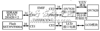
Figure 1 DSP video capture processing system overall structure block diagram
OV7620 is a CMOS color/black and white image sensor produced by OmniVision. It is configured as 16-bit progressive scan QVGA mode in this system, RGB raw data output, resolution is 320 & TImes; 240, SCCB bus, internal default line exposure mode; At the same time, the HREF signal is enabled to gate PCLK, that is, the pixel clock signal is output to the PCLK pin only when HREF is active, otherwise the pin remains inactive. This allows EDMA to be always enabled, simplifying the acquisition process. 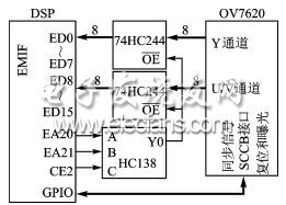
Figure 2 OV7620 and DSP hardware connection block diagram 
Table 1 Correspondence between OV7620 synchronization and control signals and GPIO
/*VSYNCGPIO6 frame sync interrupt*/
EDMA_OpenCha(PCLK_EDMA_CHANL);
/*Open the EDMA channel and prepare the OV7620 data to move */
EER&=~(1< /*Off EDMA enable, give up the data of the first HREF*/
ICR=HREF_INT_CHANL;
/ * Clear HREF (GPIO7) INT7 interrupt flag * /
IER|=HREF_INT_CHANL;
/*Enable HREF(GPIO7)INT7 interrupt*/
}
interruptvoidINT7_EXT7(void){
/*HREFGPIO7 horizontal reference interrupt*/
If(!HREF_Data_Switch){
HREF_Data_Switch=TRUE;
/*The next HREF data is valid*/
(*(EDMA_PARAM_POINTER+PCLK_EDMA_
CHANL)).CNT=IMAGESIZE_WIDTH;
/ * Correct EDMA transmission parameter count value * /
ECR|=1< /* Clear PCLK trigger event left in the cycle*/
EER|=1< /*Enable EDMA, start reading the next line of data*/
}
Else{
HREF_Data_Switch=FALSE;
/*The next HREF data is invalid*/
EER&=~(1< /* prohibits EDMA, then HREF data is not read*/
}
}