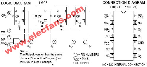
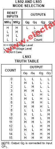
The 74LS93 is a 4-bit binary ripple counter IC commonly used in digital circuits. It consists of four flip-flops connected in a cascaded manner, allowing it to count from 0 to 15 in binary. Understanding its pin configuration and truth table is essential for proper integration into electronic designs. Below is the pin diagram of the 74LS93: Here is the truth table for the 74LS93: The truth table shows the output states of the four flip-flops (Q0 to Q3) based on the number of clock pulses applied. The counter resets when the MR pin is pulled low, returning all outputs to zero. This IC is widely used in applications such as frequency division, timing circuits, and digital counters. On Counter Scanner,Desktop Qr Code Reader Mac,Desktop Barcode Reader T97,C2 Qr Code Desktop Reader Guangzhou Winson Information Technology Co., Ltd. , https://www.barcodescanner-2d.com