The application of linear CCD in the field of image sensing and measurement technology is very rapid. In order to meet the engineering needs of adaptive measurement, a single coaxial cable bidirectional time-division multiplexing transmission external bus based on linear array CCD was designed.
In the data acquisition and measurement system, the maximum amplitude of the CCD video signal needs to be adjusted to the full scale of the ADC. There are three determinants of the maximum amplitude of the CCD signal: the photoelectric sensitivity of the CCD device, the light integration time and the illuminance. After selecting the CCD device, the value depends only on the light integration time and illuminance.

In different work sites and different periods of the work site, the light intensity often changes. If the light integration time of the CCD device is fixed, the change in illumination will cause the amplitude of the CCD video output signal to change. What is actually desired is that in the case of varying illuminance, the maximum amplitude of the video output signal should be kept stable, which can be achieved by adaptive control of the light integration time. In the process of CCD signal binarization data processing and pixel subdivision processing, the measurement information of the detected object in a frame of data is often at the boundary feature and the maximum position of the amplitude of the pixel signal, so the change of the light integration time is not The impact is measured statically.
1 Introduction to CCD device driver
Now take TOSHIBA's TCDl501C as an example, its driving pulse waveform is shown in Figure 1.
When the SH signal is low, the potential well under the Φ1 (including Φ1O and Φ1E) electrode is isolated from the storage gate potential well, and the CCD is in the light integration state; when SH is high, the deep well formed under the SH electrode communicates The storage gate potential well and the potential well under the Φ1 electrode, the signal charge packets are all transferred to the shift register, and then sequentially shifted under the action of Φ1E, O, B and Φ1E, O, B pulses, and finally by the output circuit by the OS side Output.
The pulse period of SH is the optical integration time. Taking the amplitude of the pixel signal as the controlled quantity, the maximum value of the amplitude of the video output is kept at the full range of the ADC by changing the pulse period of SH, thereby achieving the adaptive control of the optical integration time.
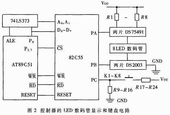
2 System composition
The acquisition system includes three parts: CCD sensor head, signal acquisition board and microcomputer. A single coaxial cable is used as a bidirectional multiplex transmission bus between the sensor head and the acquisition board, and its functional block diagram is shown in FIG. 2.
Each driving signal of CCD is generated by CPLD, and the video output passes through the driver and enters the coaxial cable. The signal acquisition board uses an ISA port and a microcomputer interface. The board uses FPGA as the logic controller of the circuit. The optical integration pulse is generated by the FPGA, and its period adjustment is controlled by the FPGA's VHDL software or microcomputer acquisition software. Under the control of the interface protocol, the CCD video signal and the optical integration pulse signal are bidirectional time-division multiplexed single coaxial cables as the transmission bus for signal and control.
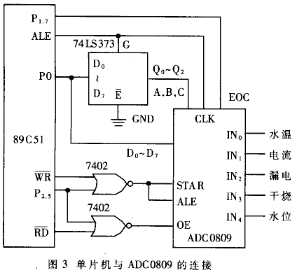
3 Principle of the electrical interface of the bus
After the crystal in the CCD sensor head is selected, the signal frequencies of Φ1 and Φ2 are also determined accordingly.  CCD pixel video signal shift output time is fixed. For example: TCDl501C has a total of 5076 pixels (in addition to 5000 exposure pixels, there are also the first 64 and the last 12 dummy), the crystal frequency is 20MHz, the CPLD output Φ1 and Φ2 frequency is 2.5MHz, the video output rate It is 5MHz, so the output time of one frame CCD signal is 5076 / 5MHz = 1.0152ms. If the optical integration time is 2ms, then in the remaining time of nearly 1ms, the CCD output is no operation, and the amplitude of the video signal is close to the clamp high level. The relationship between bus principle and control signal timing is shown in Figure 3.
In the initial state of power-on, the system sets the switch level at both ends of the coaxial cable to enable the optical integration channel. It can be seen from the timing relationship that the falling edge of the light integration pulse starts the internal logic counter of the ISA board and the CCD sensor head, and at the same time makes the switch control signal at both ends of the cable switch from the light integration channel to the CCD signal channel. Because the CCD device first outputs a certain number of dummy signals, the switching time of the selected SPDT (single pole double throw) switch is much shorter than the total output time of the previous dummy signal, so the time for the switch to switch to the CCD signal channel is The output of the exposure pixel signal has no effect. When the count reaches 5076 or 5064 (not counting the last 12 dummies), the two switch control signals at both ends of the cable change polarity again, causing the cable to switch to the optical integration pulse signal channel. In fact, as long as the channel switching is completed at any time of the empty operation before the arrival of the next optical integration pulse.
The most obvious and direct design solution was to use another standardized bus (such as the 422 bus) to exclusively transmit the light integration control signal output by the ISA board, and the CCD video signal exclusively occupies the coaxial cable, which can also meet the engineering requirements. Requirements; and the transmission distance and anti-interference performance of the 422 bus twisted pair in harsh environments is also acceptable.
However, in comparison, a single coaxial cable bidirectional multiplex bus is more advantageous.
First, the principle is more concise and practical, and its interface protocol is simpler than the 422 interface protocol;
Second, the intervention of the switch at both ends does not affect the transmission of the video signal, and the switch is switched outside the two ends of a frame of CCD signal. The transient voltage or voltage fluctuations that may occur do not affect the entire frame of the effective signal;
Third, the generation of control signals is also very convenient. Anyone familiar with VHDL or Verilog language knows that in CPLD or FPGA programming, a new counter (or originally provided with a counter) and several counting judgment control instructions are added, and an external pin is locked to output a control signal, and SPDT is realized. Switch control function;
Image 6
Fourth, the advantages of bus bandwidth and transmission distance are obvious. Compared with the 400MHz bandwidth of coaxial cable and the transmission distance of 300m ~ 500m, the twisted pair is obviously inferior;
Fifth, it saves external connection wires and is easy to install. E.g. An ISA acquisition board collects 4 CCD sensor heads. If the 422 bus interface is used to transmit optical integration pulses, 4 groups of 8 twisted pairs are required, and a single coaxial cable bidirectional time division multiplex transmission bus is used. Coaxial cable is enough, and the connection operation can not be easier;
Picture 7
Sixth, the interference resistance of coaxial cable is also better than that of twisted pair, which better meets the strict requirements of practical engineering.
Picture 8
The single coaxial cable bidirectional multiplexing transmission external bus has been applied to the data collection system of high-precision CCD angle sensor.
Detachable Earphones
Detachable Earbuds,Earphones With Detachable Cable,Earbuds With Detachable Cable,Earbuds With Replaceable Cable
Dongguang Vowsound Electronics Co., Ltd. , https://www.vowsound.com