Design of high power factor LED lighting power supply based on SEPIC converter
**1. Drive Power Topology and Control Method**
The power required to drive an LED is typically rectified from AC to DC and then directly converted. A common approach is to use a diode bridge rectifier followed by an electrolytic capacitor for filtering. However, this method results in a low power factor and introduces significant harmonic distortion into the grid. To address these issues, an active power factor correction (PFC) circuit is often employed to reduce harmonic pollution. Therefore, the power supply topology should not only achieve efficient PFC but also minimize losses.
Moreover, the size of the LED driver is usually constrained, making it essential to choose a converter that is compact, efficient, and requires fewer components. Common active PFC topologies include the BOOST, flyback, and SEPIC converters. The BOOST converter is simple and highly efficient but can only provide step-up voltage, which limits its application in scenarios where both boosting and bucking are needed. The isolated flyback converter, while capable of achieving PFC and offering both step-up and step-down capabilities, suffers from lower core utilization and efficiency due to the need for buffer circuits.
On the other hand, the SEPIC converter offers a continuous input current, reducing the need for large input filters and eliminating the requirement for additional buffer circuits. This makes it more compact and efficient, making it a suitable choice for high-power LED drivers. As shown in Figure 1, the main circuit and control system of a high-power LED driver based on a SEPIC converter are designed to regulate the LED brightness by controlling the current through the LED.
In the circuit, the voltage across C1 represents the rectified AC voltage. R1 and MOSFET are connected in series to monitor the current flowing through the MOSFET, while R2 and the LED load are used to sample the load current. The sampled signals are compared with a reference voltage, amplified, and used to control the PWM signal that regulates the MOSFET's switching, thus adjusting the LED brightness and ensuring good power factor correction.
**2. Analysis of the SEPIC Working Principle**
The operation of the SEPIC circuit can be divided into different modes based on whether the current through D5 remains above zero. These modes include discontinuous conduction mode (DCM), continuous conduction mode (CCM), and boundary conduction mode (BCM). In BCM, PFC is achieved efficiently. The equivalent circuit during critical continuous mode is illustrated in Figure 2.
During the first working mode, when the MOSFET is turned on, the input voltage charges the inductors L1 and L2, causing their currents to increase linearly. At this stage, the output capacitor C2 supplies energy to the load. When the MOSFET turns off, the stored energy in the inductors is transferred to the load through the diode D5, allowing the current to decrease gradually.
In the second working mode, the diode conducts, and the energy stored in the inductors is released to the load. During this phase, the voltage across L1 and L2 changes, affecting the current flow. The duty cycle and switching frequency are adjusted to maintain stable output and ensure a high power factor.
To optimize performance, the control loop compensation parameters are adjusted using resistors R3, R4, and capacitors C4, C5. This ensures that the control loop bandwidth is below 20 Hz, matching the line frequency and allowing the peak current of the MOSFET to follow the line voltage waveform. This results in a sinusoidal current, improving the power factor to nearly unity.
By carefully analyzing the operating principles of the SEPIC converter, it becomes clear that it is an ideal choice for high-efficiency, high-power LED lighting systems. Its ability to operate in critical continuous mode allows for precise control over the input current, resulting in improved power factor and reduced harmonic distortion.
Product details and pic
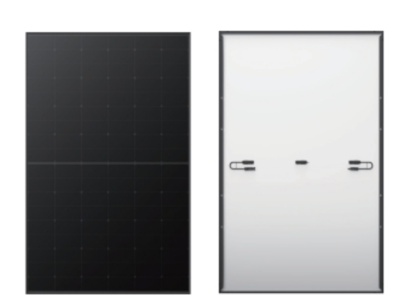
All black solar panels or black frame Solar Panel, power range around 400w to 460w which is higher solar panel efficiency the front black or front and back are both black.
All black solar panel data
| mono type | mono crystalline half cut cell |
| power range | 400watt to 460watt |
| dimensions | 1176*1134*30mm |
| type | monofacial type or bifacial type |
Product details and pic


All Black Solar Panel,Trina Solar Panel Vertex S,Mono Crystalline Pv Modules,Full Black Solar Panels 420Watt
PLIER(Suzhou) Photovoltaic Technology Co., Ltd. , https://www.pliersolar.com