Application of New HELP Technology and Switching Regulator in 3G Mobile Phones
Abstract: This paper analyzes the application of the new HELP technology and switching regulator in 3G mobile phones, and takes a new chip application as an example.
This article refers to the address: http://
1 Problem presentation and face
Today is the third generation of mobile communication (3G) era, mobile phone designers are busy developing new solutions to solve the high-speed data transmission with wcb browsing, wireless e-mail, photo and streaming video and other functions. A series of new issues. The increasing pressure is to combine these features into a shrinking enclosure that provides longer working hours. In particular, it is necessary to transmit higher power and better linearity and better efficiency. Most importantly, the phone must have longer talk time because users need to spend more time using their phone. That is to say, the increasing characteristics are realized by driving variable power at a low output voltage. However, an important factor affecting battery operating time is power efficiency and system power management. In the past, the power amplifier (PA) used to transmit signals in mobile phones was driven directly by the battery, which was simple but inefficient. The most critical aspect today is that high-speed data transmission requires higher bandwidth and transmit power. Therefore, in order to maintain a long enough battery operating time, there is now a new driving force to rethink the choice of switching regulator types. This will be an effective solution based on the unique switching regulator technology.
However, it should be specially pointed out that although the battery technology of mobile phones has been continuously improved in the past few years, it still lags behind the demand for functional expansion. To this end, designers must reduce the power consumption of mobile phones to meet the demand for high power output and longer talk time, which is achieved by semiconductor devices in mobile phones. Since the power amplifier (PA) is a component of the current huge demand, it is a very effective design solution based on the reduction of current consumption from power control, that is, high efficiency and low power (HELP) technology.
Based on the above two concepts, there are a variety of design solutions that can be applied successively. This article will take the following two new technical solutions as examples for the development of technology.
(1) A power amplifier is driven by a highly specialized step-down DC-DC switching regulator. This is a solution that is becoming more and more popular among cell phone manufacturers today. Of course, by adding an external DC/DC converter and bias voltage control, the efficiency of a single-link power amplifier at low power output can be optimized to achieve increased talk time. However, a DC/DC switching regulator technology will also increase the size and cost of the handset, which will complicate the handset design because the handset must be calibrated under different analog control conditions. So there is a second design development and application.
(2) Integrating numerous power control functions into the power amplifier module, its integrated power control function not only emphasizes the current power consumption problem, but also provides a more efficient mobile phone design method. The chip integration allows handset designers to optimize power management and achieve longer talk times without the use of separate DC/DC converters and bypass capacitors. One solution for controlling the power consumption of the power amplifier is to increase efficiency over a wide range of output powers, based on the need to optimize low power output. Because the phone works at low power levels most of the time, at about -4dBm power level. Assuming that the circuit loss between the PA and the antenna is approximately 3 dB, the output power of the PA is approximately -ldBm. At low power levels (below 0dBm), the amplifier consumes mainly quiescent current. The quiescent current of the amplifier is typically about 50 mA at -ldBm output power. By reducing the quiescent current at low power levels and increasing the efficiency of the amplifier, designers can significantly reduce power losses. However, until recently, this approach was flawed because the typical dual-state single-link PA for mobile phones was only optimized at maximum power rating, which made the handset less efficient at low power levels.
2 Based on switching regulator technology to improve the transmission efficiency of 3G mobile phone transmission
Known from the basic architecture of state-of-the-art 3G handsets, its ever-increasing features place new demands on variable power drives. For applications such as image processing, up to 360mW of power is required during video capture, which quickly drains the battery's energy. Therefore, power efficiency and system power management have become an important factor affecting the battery. Due to the heat generated during the power conversion process, it is the inevitable introduction of the unique switching regulator technology. Switching regulators with new driving forces and high efficiency are now available. This is an example of a low-noise switching regulator with a spread spectrum technology and a low-dropout, pulse-width-modulated DC-DC buck switching regulator, to analyze the design of the mobile phone's transmission efficiency.
2.1 Low noise switching regulator using spread spectrum technology
In state-of-the-art 3G handsets, all components are so dense that there is no such possibility of serious noise interference. Moreover, due to cost and size reasons, it is unrealistic to take shielding measures. One of the costs of using a switching regulator is that it is possible to generate harmonic noise. One technique that has been successfully used is to make the system clock of the DC/DC converter pseudo-random jitter. This force method and its implemented spread spectrum operation cause the switching frequency to be modulated by a pseudo random number (PRN) sequence to reduce Narrowband harmonics. This is actually "dispersing" the noise over the entire frequency range, rather than focusing on the individual harmonics. Since the peak limit of the spread spectrum noise is much lower, the interference can be greatly reduced. Although this approach has been successfully implemented with discrete components in the past, process improvements have allowed spread spectrum technology to be included in "updated" DC/DC converters, saving significant space. Take the LTC3251 switching regulator as an example.
An IC LTC3251 that achieves spread-spectrum operation on a chip is a high-efficiency, low-noise and inductorless step-down DC/DC converter with an output current of 500mA. The LTC325l's spread-spectrum oscillator is designed to generate clock pulses with a frequency between 1MHz and 1.6MHz with a randomly varying period, which has the benefit of spreading the switching noise over the entire frequency range. Figure 1 shows the function and application of the LTC3251 pin.
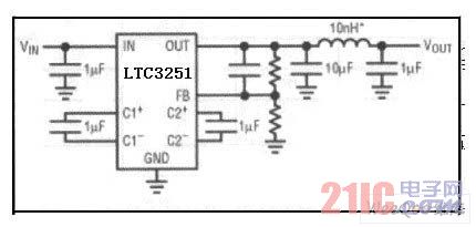
Figure 1 shows the LTC3251 pin function and application diagram.
The switching regulator avoids the efficiency limitations of linear regulators and provides up to 96% conversion efficiency through low-impedance switches and a magnetic storage component, which greatly reduces power loss during conversion. By operating at higher switching frequencies (eg, greater than 2 MHz), the size of external inductors and capacitors can be extremely reduced. The switching regulator is a very effective system power management for the latest 3G handsets, such as application processors for image processing.
2.2 Scheme for improving transmission efficiency with low dropout, pulse width modulation (PWM) DC-DC buck converter
(1) The low-dropout, pulse-width-modulated (PWM) DC-DC buck converter, the MAX1821, can be designed for WCDMA handset power amplifiers (PAs). Of course, it can also be used in other applications where high efficiency is a priority. The supply voltage range is 2.6V to 5.5V, ensuring an output current of 600mA. The 1MHz PWM switching frequency allows the use of small external components. The frequency hopping mode reduces the light load quiescent current to 180?A. The MAX1821 is dynamically controlled to provide an output voltage range of 0.4V to 3.4V. The circuit is designed to ensure an output voltage of <30?s over the full range of voltage and current. The MAX1821 sets the output voltage through an external resistor and provides a fixed output voltage range of 1.25V to 5.5V.
The MAX1821 features an internal MOSFET switch with low on-resistance and a synchronous rectifier that greatly improves conversion efficiency and reduces external component count. The 100% duty cycle allows a dropout of only 150mV at 600mA load (including external inductor resistance). . Figure 2(a) shows a block diagram of a design based on switching regulator technology to improve transmission efficiency.
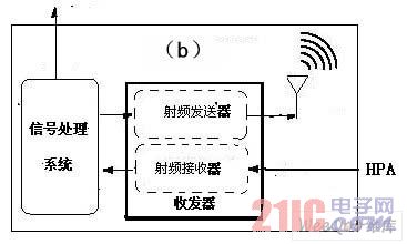
Figure 2 (a) Design block diagram based on switching regulator technology to improve transmission efficiency, (b) Base Transceiver System (BTS) components
Base Transceiver System (BTS) components include antennas, radio transceivers, signal processing systems, and support, control hardware, and software, as shown in Figure 2(b).
For wide area cellular stations, the receiver is typically connected to the antenna via a dual top module and a tower top component. The tower top component consists of a low noise amplifier (LNA) with a high power amplifier (HPA) feed forward at the transmitter antenna. As can be seen from Figure 2(a), the MAX1821 step-down switching regulator is actually embedded in the battery and WCDMA power amplifier (PA). It also constitutes a 1MHZ pulse-width-modulated buck converter with a PWM switching frequency of 1MHZ.
(2) Switching regulator is optimized for WCDMA power amplifier, which is beneficial to improve transmission efficiency.
In fact, the focus is on analyzing the special performance of the special-purpose MAX1820 switching regulator from the perspective of system performance, so that the operation of the optimized configuration is also obvious.
It can be clearly seen from Fig. 2(a) that the high-efficiency switching regulator such as the MAX1821 can dynamically adjust the supply voltage of the WCDMA power amplifier and change it according to the transmission power of the power amplifier, just enough to meet the RF signal. Amplitude requirements. It can improve the utilization of power and reduce power waste. This regulation is implemented efficiently with a switching regulator, which greatly saves battery power under any operating conditions other than peak transmit power, as shown in Figure 3.
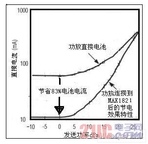
Figure 3 high efficiency switching regulator greatly saves battery power
Because the peak power is only needed when the phone is away from the base station / or data transmission. Overall, the power saving effect of this solution is very significant. If the power supply voltage of the power amplifier can be dynamically adjusted in a wide enough range, it is possible to use a fixed-gain linear power amplifier, eliminating the bias control that is currently widely used in the 3G era.
(3) Power amplifier as a load and its characteristics
From the load curve of the fixed-gain WCDMA power amplifier of the bipolar process, at the peak transmit power, the power requires a supply voltage of 3.4V and consumes 300 mA to 600 mA. At the lowest transmit power, that is, when the base station is close to the base station and only the voice is transmitted, the power amplifier draws only 30 mA of current and 0.4 V to 1 V of supply voltage. The corresponding power consumption of the power amplifier is 2040mW (maximum value) and 12mW (minimum value). Optimizing the switching regulator is not an easy task for power amplifiers with this type of load characteristics, and the MAX1821 WCDMA cellular phone step-down regulator meets this requirement.
In addition to the above, the special features of the MAX1821 that distinguish it from other types of switching regulators are as follows:
One is high efficiency over a wide load range. Without high efficiency, switching regulators lose their meaning. Therefore, high efficiency and power saving are the dominant design ideas of the MAX1821. The second is the rapid transition and establishment of the output voltage (30μs).
In the WCDMA system architecture, the transmit power needs to be adjusted 1 dB up or down every 666 μs according to the requirements of the base station to follow the transmit power level of the WCDMA power amplifier. In addition, every 10ms, the phone will have a large transmission power jump. The third is stable operation from 9.5% to 100% PWM duty cycle and low dropout voltage. Assuming that the phone is powered by a single-cell Li-Ion battery (4.2V-2.7V), the input switching regulator's voltage range is approximately 4.2v to 2.7v. In order to obtain a predictable noise spectrum and low output ripple, constant current should be used. The switching frequency of the MAX1821's forced PWM mode of operation stabilizes the duty cycle as low as 9.5% when the battery is fully charged to 4.2V and requires a power supply voltage of 0.4V.
3 Based on HELP technology can improve the power saving scheme of mobile communication terminal
3.1 HELP technology
HELP technology integrates power control functions into the power amplifier module and is the implementation of semiconductor integrated InGaP-Plus technology.
Its ANADIGICS InGaP-Plus technology solves the power amplifier optimization problem by designing a power amplifier using multiple gain links. This technology allows high performance RF switches and power amplifiers to be optimized on the same crystal. Using this technology, the first 3x3mm single-frequency (such as AWT*1) and 3x5mm dual-band (such as AWT6221) WCDMA low-power high-efficiency power amplifiers are provided. Allows the amplifier to be independently optimized at different power levels. With ANADIGICS' HELP technology, low power consumption is achieved without the need for an external voltage regulator or DC/DC converter. The InGaP-P1us technology is integrated with a virtual eutectic high electron mobility FET (the GS/D FET shown in the left of Figure 4) and a heterojunction bipolar transistor (the EBC bipolar transistor shown in the right of Figure 4). On a single chip, multi-level optimization of the two-way power amplifier is realized. The multi-level optimization of the two-way power amplifier is specifically analyzed as follows.
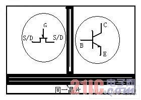
Figure 4 is a schematic diagram of HELP (high efficiency and low power) technology
Combining high-performance RF switches on the same crystal, the process can be used to design amplifiers with multiple gain links and independent linearity and efficiency optimization for each gain link. InGaP-Plus technology is designed to achieve low-power and high-efficiency power amplifiers with a dual-state (high-power and low-power) amplifier. Its InGaP-Plus technology amplifiers are optimized for high power and low power internally.
Used in InGaP-Plus technology to design a low-power, high-efficiency type 3 (HELP3) amplifier that extends handset talk time by more than 25% through internal optimization. Of course, like a single-link amplifier, you can also save more current with an external DC/DC converter. But the extra current savings are not worth it, compared to the increased cost and board area.
The low-power, high-efficiency 3-type power amplifier has specifically introduced a three-gain state that allows three different power levels to be optimized separately. For example, a high power gain (typically about 28 dBm), a *dB gain of 16 dBm, and a low power gain of 7 dBm can be optimized. This process achieves a quiescent current of less than 7 mA at low power levels, which is much less than the typical 50 mA quiescent current in a single link amplifier.
3.2 Example of quiescent current and efficiency comparison data of WCDMA power amplifier module using InGaP-Plus technology
The two models, AWT*1 and AWT6221R, are based on advanced InGaP-Plus technology and have good performances such as reliable quality, stable temperature and good durability.
(1) AWT*1 is a dual mode of operation. Provides optimum performance at high power and medium/low power output, shutdown mode and low drain voltage design, increasing handset talk and standby time. Its self-contained 3mm x 3mm x 1mm surface package includes paired network optimized output power, 50Ω system efficiency and linearity. AWT*1 is band 1, low power (16dBm) quiescent current (ICQ) and efficiency is 7mA/24%, and the size is 3×3mm.
(2) The AWT6221R product is laid out for the needs of the mobile phone industry Cingular's North American WCDMA dual-mode cellular network handset. 3mm x 5mm x 1mm, RoHS-compliant surface mount body with independent RF power amplification path to ensure optimal performance in both bands. Compared to two single-frequency power amplifiers, it saves 25% of the printed circuit board area. Manufacturers choose package pins to easily send VCC to power amplifiers and simple control pins for general VMODE. The AWT6221 is a band 2+5, low power (16dBm) quiescent current (ICQ) and efficiency is 7mA/18% for Band 2, Band 5 is 7mA/22%, and the size is 3×5mm.
4 Conclusion
The above is an application scheme of a HELP power amplifier using a switching type buck regulator in a power amplifier and InGaP-Plus technology, which has improved transmission efficiency and power saving effect. Of course, this solution can also be applied to other 3G standards and more different terminal devices, making the ideal of miniaturized, personalized data mobile phones and wireless mobile computing a reality.
Today's low-power, high-efficiency technology amplifiers go hand-in-hand with mobile handset manufacturers that are moving toward low-voltage logic. The new model of the HELP3 amplifier is designed with a 1.8V logic voltage. These amplifiers will provide longer talk time and further reduce quiescent current by less than 4mA.
At present, Lithium Polymer Battery is advanced rechargeable secondary battery. With cathode materia l- LiCoO2, LiMn2O ,Li(NiCoMn)O2, and anode material - C, lithium polymer battery has many merits: Good safety performance, high energy density, excellent charge retention, long cycle life, low self-discharge rate, low resistance, no memory effect and non-pollution.Lithium polymer battery is main applied for various customer electronic products, such as phone, smart security products, POS machine, GPS tracker and so on.
Lithium Polymer Battery
Lithium Polymer Battery,Mobile Battery,Rechargeable Lithium Polymer Batteries,Small Lithium Polymer Battery
Ji'an Powercome New Energy Technology Co., Ltd. , https://www.expowercome.com