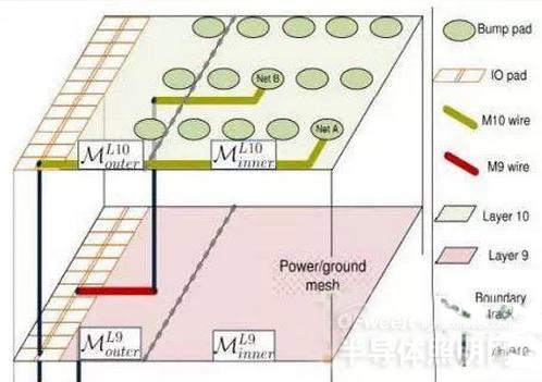
Yesterday Xiaobian has explained the "flip-chip structure and pad assignment and wiring scheme" in the method of completing the rewiring layer wiring on the pseudo-single layer, etc., and will continue to explain for you: the alternative of rewiring Framework, verification of effectiveness and other related wiring techniques. Guaranteed to pass your wiring up to 100%. Alternative framework A more practical option is the concept known as pseudo-single-layer routing, which takes up a small area on an existing metal layer (such as M9). This approach is operational and cost-effective if the occupied area is used for non-performance critical functions. In Figure 4(d), some areas of M9 (pink areas) are used to complete the routing. Here we assume that the area between the boundary line (the gray line of the dot) and the die boundary is used for auxiliary wiring. The pseudo single layer wiring method avoids cost issues and reduces the difficulty of crowded wiring. Although the foregoing work has focused on single layer wiring, the pseudo single layer wiring uses two layers of wiring in a small area. This method is suitable for rewiring layers because M9 is typically used to connect power grounds and I/O pads, and the most important M9 function is to evenly distribute power to each logic gate in the core. As a result, the importance of the peripheral area of ​​M9 is not as high as that of the central area, so that the signal network can share the peripheral area of ​​M9 with the network of the power supply. Figure 5: First and second rewiring layers on the 9th and 10th layers, respectively. The power ground is placed in M_inner^L9. The area that can be routed is M_outer^L10∪M_inner^L10∪M_outer^L9. The problem of rewiring layer wiring is manifested in the network Ni connecting the bump pad Bi and the input/output pad Oi. The first and second rewiring layers are M9 and M10, respectively, see Figure 5. We named this area as an internal/external area based on the boundary line. The entire rewiring layer is divided into four zones: M_inner^L9, M_outer^L9, M_inner^L10, and M_outer^L10. Definition of Terms â— Layout area (pseudo-single layer): M_outer^L10∪M_inner^L10∪M_outer^L9 â—External area: M_outer^L10∪M_outer^L9 â—Internal area: M_inner^L9∪M_inner^L10
LED Tunnel Lamp is an attractive, functional and weather-resistant feature.Tunnel lamps and lanterns;Die casting aluminum process and aluminum alloy forming process;Strong structure and strong impact resistance;The heat dissipation performance can guarantee the permanent work of lamps in the harsh working environment of the tunnel.Efficient and reliable constant current.Power supply can make lamps work stable and live longer;This lamp also can serve as gas station illume, charge.Station lighting and other ceiling working environment.
Led Tunnel Lamp,Rapidcure Led Tunnel Lamp,Smart Tunnel Led Lamp,Led Lamp Jiangsu chengxu Electric Group Co., Ltd , https://www.chengxulighting.com