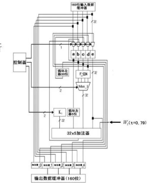
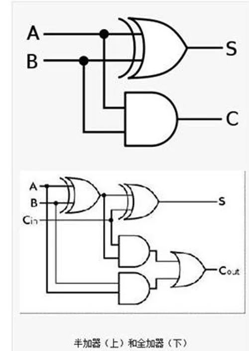
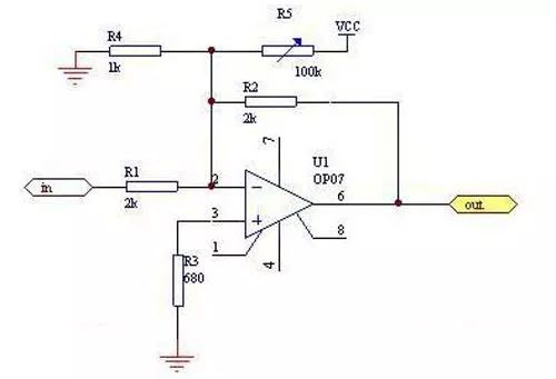
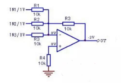
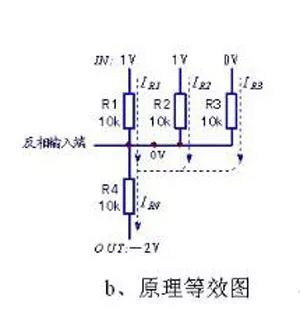
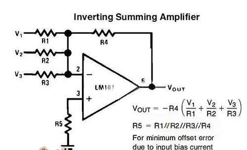
The adder is for addition. That is, the device that produces the sum of the numbers. The addend and the addend are inputs, and the sum and carry are outputs. If the addend, the addend and the low carry are the inputs, and the sum and carry are the outputs, then the full adder. Often used as a computer arithmetic logic component to perform logical operations, shifts, and instruction calls. For a 1-bit binary addition, there are five related quantities: 1, an addend A, a 2, an addend B, a 3, a carry CIN of the previous bit, 4, and a sum S of the two digits of the bit, 5. This bit adds the carry COUT generated by the two numbers. The first three quantities are the input quantity, the last two quantities are the output quantity, and the five quantities are all 1 bit. For 32-bit binary addition, there are also five related quantities: 1, addendum A (32 bits), 2, addend B (32 bits), 3, carry carry CIN (1 bit), 4 The sum of the two digits is summed with S (32 bits), 5, and the two digits of this bit are added to the carry COUT (1 bit). To achieve a 32-bit binary addition, a natural idea is to repeat the 1-bit binary addition 32 times (ie, the bitwise carry adder). This is undoubtedly feasible and easy to do, but since each CIN is provided by the previous COUT, the second bit must be calculated in the first place before the calculation can be started; the third bit must be After calculating the result in the second place, the calculation can be started, and so on. The last 32nd digit must be calculated in the first 31 positions before the calculation can begin. Such a method makes the time required to implement a 32-bit binary addition to be 32 times the time to implement a 1-bit binary addition. basic method It can be seen that the upper method is to serially add 32 bits of 1 bit and 1 bit. To shorten the time of the process, it is necessary to try to parallelize the process of the above. Types of In terms of the unit adder, there are two basic types: a half adder and a full adder. The half adder has two inputs and two outputs. The inputs can be identified as A, B or X, Y. The outputs are usually identified as S and C. A and B are S after XOR operation and C after AND operation. The full adder introduces the input of the hexadecimal value to calculate the larger number. To distinguish the two hexadecimal lines of the full adder, the input is denoted as Ci or Cin, and the output is denoted as Co or Cout. The half adder is abbreviated as HA, and the full adder is abbreviated as FA. Half adder: Half adder circuit diagram The half adder has two binary inputs that add the values ​​entered and output the result to (Sum) and hex (Carry). Although the half adder can generate a hexadecimal value, the half adder itself cannot process the hexadecimal value. Full adder: The full adder has three binary inputs, one of which is the input of the hexadecimal value, so the full adder can process the hexadecimal value. The full adder can be combined with two half adders. Note that the last OR gate of the hex output can also be replaced with an XOR gate and there is no need to change the rest. Because the OR gate and the XOR gate only differ when the inputs are all 1, and this possibility no longer exists. Second, the principle of the adder Let the input of the ith bit of an n-bit adder be ai, bi, ci, and output si and ci+1, where ci is the carry of the lower bit, ci+1 (i=n-1, n-2,..., 1,0) is the carry to the upper, c0 is the carry input of the entire adder, and cn is the carry output of the entire adder. And Si=aiii+ibii+iici+aibici, (1) carry ci+1=aibi+aici+bici, (2) Let gi=aibi, (3) Pi=ai+bi, (4) Then ci+1= gi+pici, (5) As long as aibi=1, a carry to i+1 bit is generated, and g is called a carry generation function; likewise, as long as ai+bi=1, ci is passed to i+1 bit, so p is called carry transfer function. . Expand equation (5) to get: ci+1= gi+ pigi-1+pipi-1gi-2+...+ pipi-1...p1g0+ pipi-1...p0c0(6) . As the number of bits increases, the equation (6) is lengthened, but the depth of the three logic levels is always maintained, so the delay for forming the carry is a constant independent of the number of bits. Once the carry (c1~cn-1) is calculated, the sum can be derived from equation (1). The adder that uses the above formula to generate all carry in parallel is the carry-forward adder. Generating gi and pi requires a first-level gate delay, ci requires two levels, and si requires two levels, requiring a total of five levels of gate delay. Compared with the series adder (generally 2n-level gate delay), the delay time of the super-advanced adder is greatly shortened (especially when n is relatively large). Third, the inverse principle of the inverse adder The inverting adder circuit, also known as the inverting summing circuit, means that more than one input signal enters the inverting input terminal, and the output result is the absolute value of the multi-channel signal addition (the opposite voltage polarity). As shown in the circuit a, when R1=R2=R3=R4, its output voltage = the absolute value of IN1+IN2+IN3, which constitutes the inverting adder circuit. When R4 "R1", the circuit has both signal amplification. Inverted adder and principle equivalent diagram The basic circuit structure of the inverting adder is an inverting amplifier, and its "virtual ground" characteristic shows that both input terminals are at 0V ground potential. This determines the purpose of the control of the circuit, so that the potential of the inverting input is 0V (the target value of the non-inverting input is 0V). The circuit circuit parameters and input signal values ​​of the above diagram a are analyzed, and the equivalent diagram shown in the above figure b can be obtained. The bias circuit of the inverting adder is still in the form of a series divided circuit, but the input circuit also involves the circuit principle of parallel shunting of the resistor. The equation can be listed as IR4=IR1+IR2+IR3. The "confidential" of the inverting adder is thus disclosed. Since the inverting input terminal is ground potential 0V, when the input signal IN3=0V, no signal current is generated in the branch, which is equivalent to no signal input, thereby becoming IN1+IN2=-OUT. When IR1(1V/10k)=0.1mA, IR2(1V/10k)=0.1mA, the condition of IR4=IR1+IR2 is satisfied only when the OUT output is -2V. If the principle equivalent diagram is further simplified (see the c circuit in the figure), a very familiar figure will be reflected in our mind: Is this not an inverting amplifier circuit? Yes, yes, reverse phase summation The (inverting adder) circuit is the inverting (including amplification and attenuation). In practical applications, due to the obvious defects of the in-phase adder, the input input impedance is extremely high, and the signal input current can only be self-formed through multiple IN terminals (which will cause the input signal voltage to be involved in each other and cause large operation errors) Unless the internal resistance of various IN sources is very small, it will not affect the calculation accuracy. Therefore, the application is less. Due to its "virtual ground" characteristic, the inverting summing circuit has a very low input impedance, so that the input signal current of each channel enters the input terminal in the "convergence mode", and does not cause current flow between the input signals, so the operation precision can be guaranteed. , more applications. Fourth, the inverse phase adder circuit and principle (Figure)
The RIMA 12V AGM Battery is part of our UN series sealed lead acid battery,
UN series is a high quality lead acid battery, made of 99.997% pure lead, the battery is perfect designed for standby use, but also good at cycle use. The battery is based on AGM battery technology, which means that the electrolyte is absorbed by a fiberglass separator, preventing its leakage, this way the battery can work in any positions.
General Future:
5-12 years design life(25℃)
Non-spillable construction
Sealed and maintenance-free
High reliability and stability
High purity raw material: long life and low self-discharge
Standards:
Compliance with IEC, BS, JIS and EU standards.
UL, CE Certified
ISO45001,ISO 9001 and ISO 14001 certified production facilities
Application:
Uninterruptible Power Supply (UPS)
Emergency backup power supply
Auto control system
Communication power supply
Alarm and security system
Electric Power System (EPS)
12V Battery Rechargeable,12V Battery Small,12V Battery 12Ah,Sealed Lead Acid 12V Battery OREMA POWER CO., LTD. , https://www.oremabattery.com